
There’s still plenty of room at the bottom to generate piezoelectricity. Engineers at Rice University and their colleagues are showing the way.
A new study describes the discovery of piezoelectricity—the phenomenon by which mechanical energy turns into electrical energy—across phase boundaries of two-dimensional materials.




The work was led by Rice materials scientists Pulickel Ajayan and Hanyu Zhu and their colleagues at Rice’s George R. Brown School of Engineering, the University of Southern California, the University of Houston, Wright-Patterson Air Force Base Research Laboratory, and Pennsylvania State University.
The discovery could aid in the development of ever-smaller nanoelectromechanical systems, devices that could be used, for example, to power tiny actuators and implantable biosensors, and ultrasensitive temperature or pressure sensors.
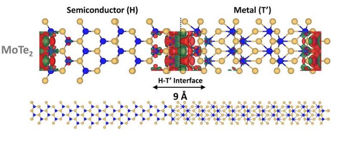
The researchers show the atomically thin system of a metallic domain surrounding semiconducting islands creates a mechanical response in the material’s crystal lattice when subjected to an applied voltage.
The presence of piezoelectricity in 2D materials often depends on the number of layers, but synthesizing the materials with a precise number of layers has been a formidable challenge, said Rice research scientist Anand Puthirath.
“Our question was how to make a structure that is piezoelectric at multiple thickness levels—monolayer, bilayer, trilayer, and even bulk—from even non-piezoelectric material,” Puthirath said. “The plausible answer was to make a one-dimensional, metal-semiconductor junction in a 2D heterostructure, thus introducing crystallographic as well as charge asymmetry at the junction.”
“The lateral junction between phases is very interesting, since it provides atomically sharp boundaries in atomically thin layers, something our group pioneered almost a decade before,” Ajayan said. “This allows one to engineer materials in 2D to create device architectures that could be unique in electronic applications.”
The junction is less than 10 nanometers thick and forms when tellurium gas is introduced while molybdenum metal forms a film on silicon dioxide in a chemical vapor deposition furnace. This process creates islands of semiconducting molybdenum telluride phases in the sea of metallic phases.
Applying voltage to the junction via the tip of a piezoresponse force microscope generates a mechanical response. That also carefully measures the strength of piezoelectricity created at the junction.
“The difference between the lattice structures and electrical conductivity creates asymmetry at the phase boundary that is essentially independent of the thickness,” Puthirath said. That simplifies the preparation of 2D crystals for applications like miniaturized actuators.
“A heterostructure interface allows much more freedom for engineering materials properties than a bulk single compound,” Zhu said. “Although the asymmetry only exists at the nanoscale, it may significantly influence macroscopic electrical or optical phenomena, which are often dominated by the interface.”

