Cornell engineers and materials scientists have added a state-of-the-art tool to their suite of laboratory equipment to help in the study of gallium oxide, a material commonly viewed as the heir apparent to silicon carbide and gallium nitride as the go-to semiconductor for many power electronics applications.
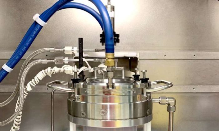
An Agnitron Agilis 100 metal-organic chemical vapor deposition (MOCVD) system began operating on June 30 in the Duffield Hall laboratory of Hari Nair, assistant research professor of materials science and engineering. It has been specifically calibrated to create thin films of gallium oxide, a semiconductor material prized for its ability to handle high voltages, power densities, and frequencies. Those attributes make it an ideal material for electric vehicles, renewable energy sources, and 5G communications, among other applications.


“Another key advantage of gallium oxide is the ability to grow single crystals of this material from its molten form,” Nair said, “which will be key for scaling up the substrate size. This capability to scaling up is very important for industry adoption of electronic devices made using new semiconductor materials.”
The gallium oxide MOCVD systems work by spraying a metal-organic gallium precursor over a heated single crystalline semiconductor substrate. The heat causes the precursor to decompose, freeing gallium atoms that then bond with oxygen atoms on the surface of the wafer, resulting in a high-quality crystalline layer of gallium oxide.
MOCVD is the industry standard for producing epitaxial thin films of compound semiconductors such as group III-arsenides, group III-phosphides, and group III-nitrides, which play a significant role in optical and mobile communications, as well as solid-state lighting, among other applications. Over the past five years, the quality of gallium oxide grown using MOCVD has steadily improved.
“With this system, we can grow thin films on up to 2-inch-diameter substrates under widely tunable oxidation chemical potentials,” said Nair. “It also has a very high substrate temperature capability and we can heat the substrate up to 1,500 degrees Celsius. High substrate temperatures yield better quality films which are key for pushing the performance of electronic devices.”
Nair plans to collaborate with researchers from the AFRL-Cornell Center for Epitaxial Solutions and elsewhere on campus to optimize MOCVD for gallium oxide, which would make the material more economically attractive to manufacturers looking for high-precision, high-volume production.
“There is a need to make power electronics more compact and more efficient,” Nair said. “One of the dreams is to take a power substation, which is about the size of a small house, and shrink it down to the size of a suitcase. Such innovations will be key for creating a smart power grid, and gallium oxide semiconductor-based power electronics is a stepping stone in making this possible.”
“The wide bandgap offered by gallium oxide is great, but if you cannot grow this on large area substrates, then it’s a showstopper from a practical point of view,” Nair said. “There’s a big promise gallium oxide has to offer, but we’re not there yet.”