
Semicon 2.0 is the next phase of India Semiconductor Mission (ISM) approved by the Union Cabinet with the primary goal of expanding domestic chip design, manufacturing, advanced packaging, research and talent development. Prime Minister Narendra Modi highlighted the transition to Semicon 2.0 by stating the ambition of the semiconductor ecosystem that “India’s chip will go out to the world” as India is emerging as a major source of developing semiconductor value chain.
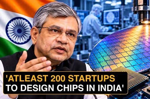
Under Semicon 2.0, the government is targeting at least 200 startups and companies involved in chip design in India to scale up domestic semiconductor capabilities. This will build momentum with already 105 startups who have started developing chips and received access to industry-grade EDA tools. Electronics and IT Minister Ashwini Vaishnaw at SEMOCON India, 2026 said that 20 of those 105 startups have secured venture-capital funding, and the government wants to expand this ecosystem to at least 200 startups and companies.




The programme is structured into six broad focus areas covering chip design, semiconductor machinery and materials, additional fabrication facilities, advanced packaging and testing, research and development, and talent development. This approach aims to take India’s semiconductor ecosystem beyond the initial foundation created under Semicon 1.0 to a more complete production facility.
Talent development is another major focus of this initiative. The IT Minister also stated that around 70,000 semiconductor design engineers have been trained as part of India’s accelerated talent development to strengthen its home-grown chip-design ecosystem under the India Semiconductor Mission.

