As resolution and sample rates continue to rise for ADCs, the driver circuitry for the analog inputs, not the ADC itself, has increasingly become the limiting factor in determining overall circuit accuracy. Beyond a simple 1-pole RC lowpass filter (LPF1) for noisy input signals (Figure 1), a coupling RC filter network (LPF2) is often used between the buffer and ADC input to minimize disturbances reflected into the buffer from ADC sampling transients. Long RC time constants at the analog inputs slow the settling of these disturbances. Therefore, LPF2 typically requires a wider bandwidth than LPF1. This filter also helps minimize the noise contribution from the buffer.
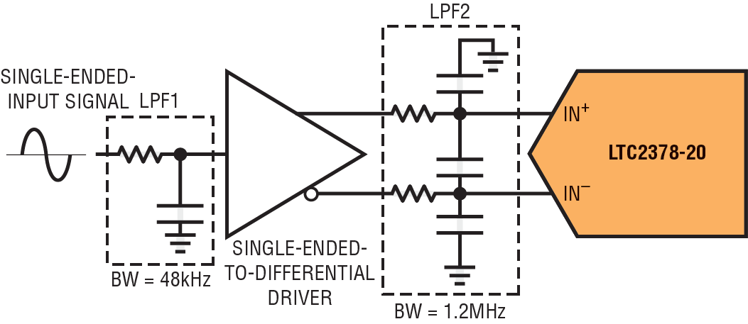




Figure 1. Simulating the interface between an amplifier and ADC can help determine trade-offs between noise and settling time.
Simulating the interface between the amplifier and ADC presents some interesting trade-offs between settling time and noise performance. Experimenting with such simulations helps one develop an intuitive understanding of how the filter design affects these performance aspects.
The analog input of a fully differential SAR ADC can be modeled as a switched capacitor load on the drive circuit shown in equivalent form in Figure 2. The values shown are from the LTC2378-20 20-bit, 1Msps, low power SAR ADC but can easily be modified to represent other ADCs. During the acquisition phase, each input sees approximately 45pF (CIN) from the sampling CDAC in series with 40Ω (RON) from the ON-resistance of the sampling switch. The inputs draw a current spike while charging the CIN capacitors in this phase. During the subsequent conversion phase, the analog inputs draw only a small leakage current and the capacitors are fully discharged. This modeling of the ADC analog input highlights one of the biggest challenges in coupling an amplifier to a SAR ADC such as the LTC2378-20; dealing with current spikes drawn by the ADC inputs at the start of each acquisition phase.
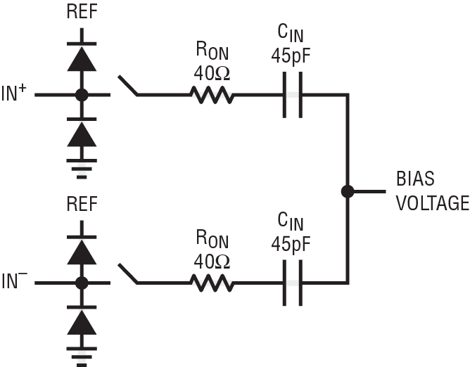
Figure 2. Equivalent circuit for the analog input of the SAR ADC.
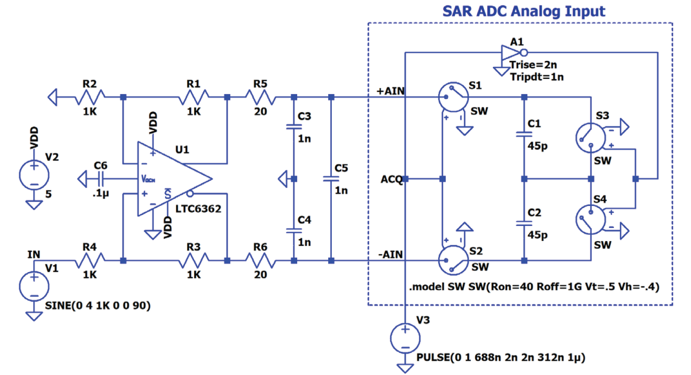
A simulation schematic of this equivalent circuit is shown in Figure 3. The low power LTC6362 differential op amp is configured to convert a single-ended input signal to a fully differential output to drive the LTC2378-20. To simplify the simulation, the input ESD protection diodes are not included. The two 45pF input capacitors (C1 and C2) are charged via voltage controlled switches (S1 and S2) that are defined by a SW model statement with an ON resistance of 40Ω. These switches are driven by a pulsed voltage source with a duration of 312ns and period of 1µs to simulate the acquisition time of the LTC2378-20 SAR ADC at 1Msps. To ready the sampling capacitors for the next acquisition phase, an idealized behavior inverter (A1) is used to turn on the second set of switches (S3 and S4) that discharge the capacitors.
Figure 3. Simulation schematic of SAR ADC analog input equivalent circuit.
The RC filter network between the amplifier and the ADC serves several purposes. First, the filter network reduces the amount of wideband noise entering the ADC. Second, the capacitors serve as a charge reservoir to absorb charge kickback from the ADC’s internal sampling capacitors. After each conversion cycle, the discharged sample capacitors (45pF) are reconnected to the amplifier circuit. By placing a much larger reservoir capacitor at the ADC input, the voltage excursion caused by these sample capacitors is reduced. There is, however, a trade-off between wideband noise and settling time performance. While the sample capacitors are connected to the amplifier circuit (acquisition time), the RC network should fully settle to within the resolution of the ADC. Using too much reservoir capacitance in the filter network increases this settling time beyond acceptable limits. For further discussion of this trade-off, watch Kris Lokere’s “SAR ADC Driver Interface.”