
Kyoto, Japan, April 15, 2026 – Nuvoton Technology announced today the start of mass production of a “high-power violet laser diode (402 nm, 4.5 W) ” that achieves industry-leading class optical output in a 9.0 mm diameter CAN package (TO-9). This product achieves 1.5 times the optical output compared to our conventional product through our proprietary device structure and heat dissipation design technology, and contributes to improving production throughput in optical equipment such as maskless lithography systems. Furthermore, adding this product to our lineup enables our product portfolio to support major photosensitive materials used in advanced semiconductor packaging.
Achievements:


- Achieves 4.5 W high-power at 402 nm, 1.5 times that of our conventional product, enhancing production throughput in maskless lithography systems
- Expands our lineup of light sources for maskless lithography in advanced semiconductor packaging, supporting multiple major photosensitive materials
- Expands the lineup of mercury lamp replacement solutions [6] , providing new options in light source selection
For more product details, please see here: https://nuvoton.co.jp/semi-spt/apl/rd/?id=1100-0272
Features of New Product:
- Achieves 4.5 W high-power at 402 nm, 1.5 times that of our conventional product, enhancing production throughput in maskless lithography systems
Violet (402 nm) laser diodes generally suffer from relatively low wall-plug efficiency [7] and significant self-heating, and are also prone to short-wavelength-induced degradation, which makes stable high-power operation difficult.
To address these challenges, the “device structure that enhances wall-plug efficiency (WPE)” and the “high thermal conduction package technology that effectively dissipates heat,” which were used in the high-power ultraviolet laser diode [8] (379 nm, 1.0 W) announced as a new product in January 2026, have been expanded to the violet (402 nm) band.
As a result, we are launching a “high-power violet laser diode (402 nm, 4.5 W)” that achieves 1.5 times the optical output compared to our conventional product. In particular, by applying our proprietary facet coating technology that suppresses degradation factors at the laser facets, we have improved the lifetime performance during high-power operation, and by adopting a monolithic molded structure using high heat dissipation materials for the package, we have improved heat dissipation performance.
By achieving both “high-power” and “high reliability”, this product enhances production throughput in industrial optical equipment where high quality is required.
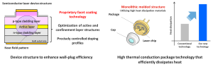
| Figure 1: “Device structure that enhances wall-plug efficiency” and “High thermal conduction package technology that effectively dissipates heat” |
- Expands our lineup of light sources for maskless lithography in advanced semiconductor packaging, supporting multiple major photosensitive materials
This product will deliver significant value in maskless lithography for advanced semiconductor packaging, a market that is rapidly growing, driven by expanding demand for artificial intelligence (AI) and other applications.
In circuit formation for advanced semiconductor packages, maskless lithography technology that directly exposes (draws) wiring patterns based on design data has been attracting attention in recent years, as it enables not only cost reduction and development period shortening, but also high-precision patterning correction in response to substrate warpage and distortion.
For laser diodes, which are one of the main light sources in this maskless lithography technology, there has been a demand for compatibility with wavelengths close to the i-line (365 nm) and h-line (405 nm), which are the emission lines of mercury lamps, in order to correspond to the main photosensitive materials, as well as higher output for the purpose of improving the production throughput of equipment.
In addition to the “high-power ultraviolet laser diode (379 nm, 1.0 W)” for i-line applications announced in January 2026, we are adding this new product, “high-power violet laser diode (402 nm, 4.5 W) “, for h-line applications to our lineup.
This expansion strengthens our lineup of light sources for maskless lithography in advanced semiconductor packaging, enabling consistent support for multiple major photosensitive materials while contributing to higher production throughput of equipment.
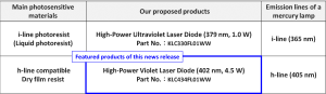
| Table 1: Major Photosensitive Materials in Maskless Lithography for Advanced Semiconductor Packages and Our Proposed Products |
- Expands the lineup of mercury lamp replacement solutions, providing new options in light source selection
This product will be newly added to the lineup of our “semiconductor laser-based alternatives to mercury lamps.” The h-line (405 nm), which is an emission line of mercury lamps, is used in a wide range of fields such as photocuring, 3D printing, sensing, biomedical applications, and marking, and this product provides customers with a new option as an alternative light source for these applications.
Furthermore, by leveraging the high-power performance that is a feature of this product, it will contribute to improving the efficiency of processes that were difficult to realize in the past, as well as to the creation of new optical applications.
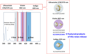
| Figure 2: “Mercury Lamp Replacement Solution Using Semiconductor Lasers” Developed by Our Company |
This product is scheduled to be exhibited at our booth at “OPIE’26” to be held in Yokohama, Japan.
Applications:
- Maskless lithography
・ Resin curing
・ Sensing
・ Marking
・ 3D printing
・ Biomedical
・ Alternative light source for mercury lamps, etc.
Product name:
KLC434FL01WW
Specifications:
| Part number | KLC434FL01WW |
| Wavelength | 402 nm |
| Optical Output Power | 4.5 W |
| Package Type | TO-9 CAN |
Start of mass production: May 2026