
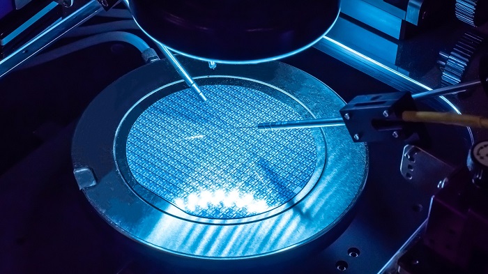
To make computer chips, technologists around the world rely on atomic layer deposition (ALD), which can create films as fine as one atom thick. Businesses commonly use ALD to make semiconductor devices, but it also has applications in solar cells, lithium batteries and other energy-related fields.
Today, manufacturers increasingly rely on ALD to make new types of films, but figuring out how to tweak the process for each new material takes time.




Part of the problem is that researchers primarily use trial and error to identify optimal growth conditions. But a recently published study—one of the first in this scientific field—suggests that using artificial intelligence (AI) can be more efficient.
In the ACS Applied Materials & Interfaces study, researchers at the U.S. Department of Energy’s (DOE) Argonne National Laboratory describe multiple AI-based approaches for optimizing the ALD processes autonomously. Their work details the relative strengths and weaknesses of each approach, as well as insights that can be used to develop new processes more efficiently and economically.
All of these algorithms provide a much faster way of converging to optimum combinations because we’re not spending time putting a sample in the reactor, taking it out, doing measurements etc. as you typically would today. Instead you have a real-time loop that connects with the reactor.
Cutting edge, but with challenges
In ALD, two different chemical vapors, known as precursors, adhere to a surface, adding a thin layer of film in the process. This all happens inside a chemical reactor and is sequential: one precursor is added and interacts with the surface, then any excess of it is removed. Afterwards the second precursor is introduced then later removed, and the process repeats itself. In microelectronics, the ALD thin film might be used to electrically insulate nearby components in nanoscale transistors.
ALD excels at growing precise, nanoscale films on complex, 3D surfaces such as the deep and narrow trenches patterned into silicon wafers to manufacture today’s computer chips. This has motivated scientists worldwide to develop new thin film ALD materials for future generations of semiconductor devices.

