Nanosheets are finely structured 2D materials and have great potential for innovation. They are fixed on top of each other in layered crystals, and must first be separated from each other so that they can be used, for example, to filter gas mixtures or for efficient gas barriers. A research team at the University of Bayreuth has now developed a gentle, environmentally-friendly process for this difficult process of delamination that can even be used on an industrial scale. This is the first time that a crystal from the technologically attractive group of zeolites has been made usable for a broad field of potential applications.
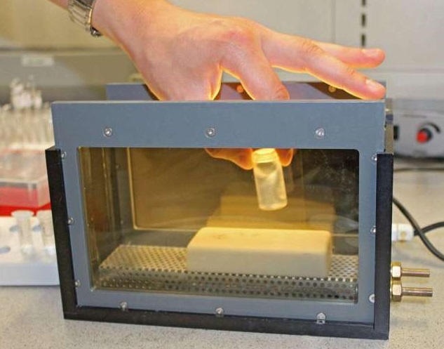
The delamination process developed in Bayreuth under the direction of Prof. Dr. Josef Breu is characterized by the fact that the structures of the nanosheets isolated from each other remain undamaged. It also has the advantage that it can be used at normal room temperature.


The 2D nanosheets, which lie on top of each other in layered crystals, are held together by electrostatic forces. In order for them to be used for technological applications, the electrostatic forces must be overcome, and the nanosheets detached from each other. A method particularly suitable for this is osmotic swelling, in which the nanosheets are forced apart by water and the molecules and ions dissolved in it. So far, however, it has only been possible to apply it to a few types of crystals, including some clay minerals, titanates, and niobates. For the group of zeolites, however, whose nanosheets are highly interesting for the production of functional membranes due to their silicate-containing fine structures, the mechanism of osmotic swelling has not yet been applicable.
The Bayreuth research team has now—for the first time in interdisciplinary collaboration—found a way to use osmotic swelling for the gentle separation of ilerite crystals, which belong to the group of zeolites. In the process, large sugar molecules are first inserted into the narrow spaces between the nanosheets. Subsequently, the nanosheets, which are stacked on top of each other and structurally aligned, are separated by water. In the process, their spacing becomes considerably larger. Now the nanosheets can be pushed further apart horizontally in different directions: Upon subsequent drying, a solid surface is created that is composed of many nanosheets. These are stacked like playing cards, overlapping only at the edges and leaving only a few gaps. The diameter of the individual nanosheets is around 9,000 times greater than their thickness.
This now opens up the possibility of fixing a larger number of such surfaces on top of each other and building up new layered materials. The point of this process is that the nanostructures of the surfaces in the new material are offset from each other. Consequently, their gaps are not exactly on top of each other, so molecules, ions, or even light signals cannot penetrate the new material directly. This labyrinthine overall structure enables a wide range of potential applications, such as in packaging used to keep food fresh, in components for optoelectronics, and possibly even in batteries.