

For decades, the semiconductor industry has been struggling with near-short defects in the wire bond of an integrated circuit (IC), without an effective solution to detect them. When two wire bonds come very close to each other but are not electrically shorted, that results in a near short condition. This presents a potential reliability issue. The insulative barrier between the wires can give way over time, or after extended stress, resulting in a catastrophic failure of the device. Depending on the IC application, such a failure can result in loss of life.
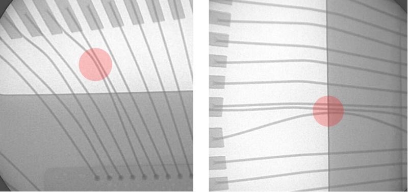




Xray imaging detects a near short in the wire bonds of an IC
Open and short circuit tests are common test methods used for all electrical test systems, including automated test equipment (ATE) systems used in the semiconductor industry. However, when two wires are not electrically shorted, this test is ineffective in catching the defect. If they are not touching each other and creating a short circuit path, you cannot detect them electrically.
The only alternative is to use X-ray inspection systems to check each of the wires, either visually or automatically. Manual visual inspection is labour intensive and highly ineffective due to human fatigue and errors. Automated inspection, on the other hand, is more reliable but has a low output rate due to the long inspection time. As both methods cannot keep up with the beat rate of the manufacturing line, manufacturers can only implement this test based on sampling, leaving the potential for defective ICs to escape detection.
Keysight’s Vectorless Test Enhanced Performance (VTEP) technology is the answer to this potential issue. VTEP is an evolution from the TestJet technology that took over the in-circuit test industries in the early 90s. VTEP evolution brings with it a better signal-to-noise ratio, which is critical in wire bonds near short testing.
VTEP technology captures open pins of the IC mounted on a printed circuit board. The technology is not new, and the theory is simple. The stimulus travels from the pin through the lead frame and up to the wire bond. Place the VTEP sensor plate on the top surface of the IC and that creates a capacitive structure between the wire bond and the sensor plate. The VTEP amplifier circuit on the sensor place measures the coupling response to derive the capacitance value. Deformations in the wire bond results in a shift of capacitance values which we can detect.
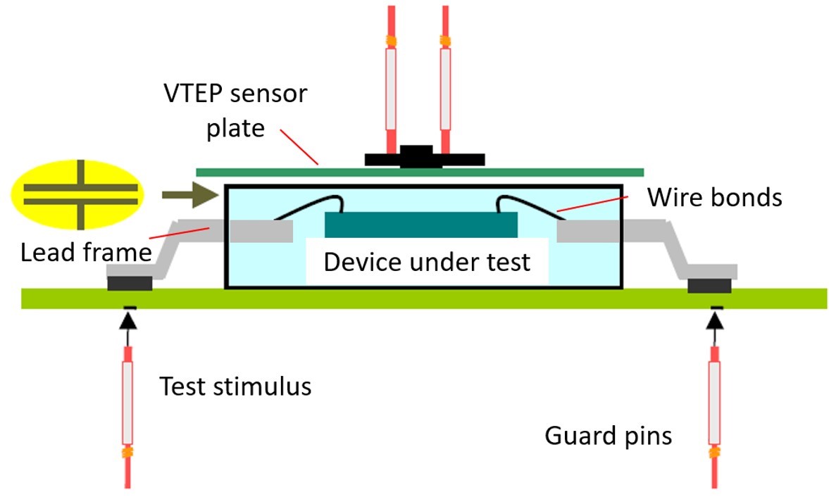
Keysight VTEP Technology
In the diagram above, the capacitive coupling happens between the lead frame, including the wire bond and the sensor plate above the IC. A shift in the wire bond position changes the distance of the dielectric layer between the stimulus and the sensor plate. This results in a very small drift in the capacitive measurement compared to others where the wire bonds are in good position.
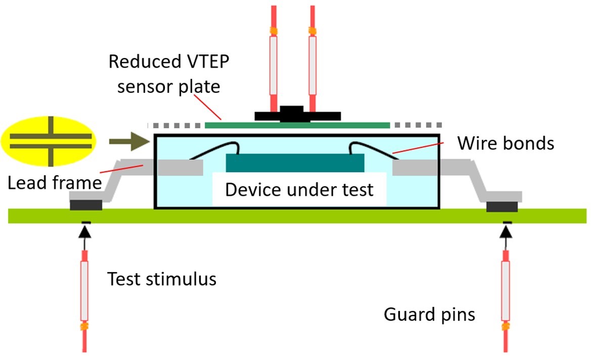
Reduce VTEP sensor plate for cover wire bond area only
The measured capacitive coupling response includes part of the lead frame and not just the wire bond. Given the large ratio in size between a lead frame and its wire bond, we can say that 80 to 90% of the measured response probably comes from the lead frame itself. This dilutes the resolution of the test as we are only interested in the wire bond in this case. Therefore, to enhance the resolution of the measurement, we can reduce the size of the sensor plate, such that it omits the lead frame area and just cover the wire bonds only.
In doing so, you see that the measurement drops to a fraction of what it was before, but the resolution of the measurement improves significantly. Combining that with VTEP’s high signal-to-noise ratio, we can now detect a shift of the wire bond’s physical position inside the encapsulation of an IC itself.
What about the speed of the VTEP test? It’s a fraction of a second! VTEP test typically measures one pin in a matter of a few milliseconds. A 100-pin IC will take less than a second to complete its test. Thus, making VTEP a viable solution to the long-standing problem of near-short defects in IC.
This takes VTEP technology into a new industry of semiconductor tests. Capacitive wire bond testing using VTEP is the only solution that addresses the near-short defect issue effectively and meets the high output rate requirement of the semiconductor manufacturing line.
Authored Article by:
Kwan Wee Lee, Technical Marketing Engineer, Keysight Technologies

