
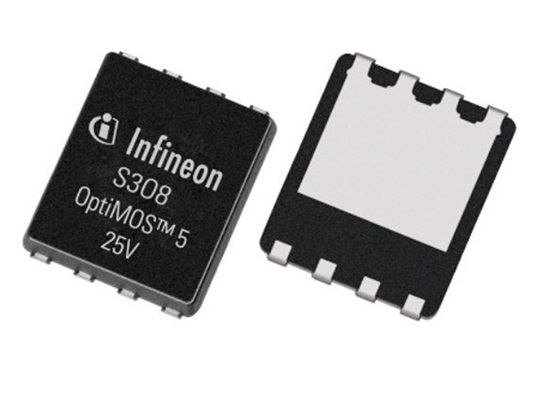
Infineon Technologies AG (FSE: IFX / OTCQX: IFNNY) is focusing on system innovation with enhancements on component level by addressing the challenges of modern power management designs.
The Source Down is the new industry standard packaging concept. The first wave of power MOSFETs launched in this new package is the OptiMOSTM 25 V in a PQFN 3.3×3.3 mm. The device sets a new industry benchmark in MOSFET performance, reducing on-state resistance (RDS(on)) and offering superior thermal management capability to the marketplace. The product is well-suited for a wide range of applications such as drives, SMPS (including server, telecom, and OR-ing) and battery management.




The new package concept connects the source potential (instead of the drain potential) to the thermal pad. Along with the enabled new PCB layout possibilities, this helps achieving ever higher power density and performance. Two different footprint versions are released – the Source-Down Standard-Gate and the Source-Down Center-Gate in a PQFN 3.3×3.3 mm package. The Source-Down Standard-Gate footprint is based on the current PQFN 3.3×3.3 mm pinout configuration.
The location of the electrical connection remains the same, simplifying the drop-in replacement of today’s standard Drain-Down packages with the new Source-Down package. For the Center-Gate version, the gate-pin is moved to the center supporting easy parallel configuration of multiple MOSFETs. With its larger drain-to-source creepage distance, it is possible to connect the gates of multiple devices on a single PCB layer. In addition, moving the gate connection to the center leads to a wider source area for improved electrical connection of devices.
This technology innovation results in major reduction of RDS(on) by up to 30 % compared to current technology. The thermal resistance between junction to case (RthJC) is also significantly improved compared to the current PQFN packages. Reduced parasitics, improved PCB losses, as well as superior thermal performance, add significant value to any contemporary engineering designs.
The OptiMOS™ Source-Down will be showcased at Infineon’s booth 1510 at the 2020 Applied Power Electronics Conference and Exposition (APEC), which takes place in New Orleans, LA from March 16-18.
Availability
Both OptiMOSTM Source-Down 25 V power MOSFETs in a PQFN 3.3×3.3 mm package are now available.
For more information, visit www.infineon.com

