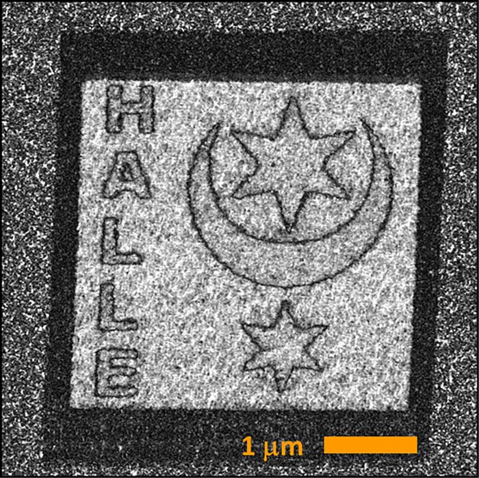
Precisely applied mechanical pressure can improve the electronic properties of a widely used polymer material. This requires that the material be mechanically processed to an accuracy of a few nanometers, a team from Martin Luther University Halle-Wittenberg (MLU). In their new study, the researchers show how this previously unknown physical effect works and how it could also be used for new storage technologies. The team has also succeeded in sketching the coat of arms of the city of Halle as an electrical pattern with a spatial resolution of 50 nanometers in the material.
Polyvinylidene fluoride (PVDF) is a polymer widely used by industry to produce seals, membranes, and packaging films. It has many practical properties as it is stretchable, biocompatible, and rather inexpensive to produce. “PVDF is also a ferroelectric material. This means it has positive and negative charges that are spatially separated, something which can be utilized for storage technology,” says physicist Professor Kathrin Dörr at MLU. However, there is a drawback: PVDF is a semi-crystalline material whose structure, unlike crystals, is not completely ordered. “There is so much disorder in the material that some of the properties that you would actually like to take advantage of are lost,” says Dörr.


Her team discovered by chance that atomic force microscopy can be used to establish a specific electric order in the material. This method usually involves scanning a material sample with a tip only a few nanometers in size. A laser is then used to measure and evaluate the produced vibrations. “This enables us to analyze the material’s surface structure at the nano level,” says Dörr. Atomic force microscopes can also be used to apply pressure to the material sample with the aid of the tiny tip. The physicists at MLU discovered that this also changes the electrical properties of the PVDF.
“The pressure elastically compresses the material at the desired point without shifting the molecules that make it up,” Dörr explains. The electrical polarization of the material (i.e., its electrical orientation) rotates in the direction of the pressure. Thus, the polarization can be controlled and reoriented at the nano level. The electrical domains created in this way are extremely stable and were still intact four years after the original experiment.
The effect discovered by the researchers from Halle can be controlled so precisely that they were able to use the electrical charges to sketch in the material a nano-sized version of the city’s coat of arms—probably the smallest in the world. The new process could help enable materials like PVDF to be used in novel electrical and storage applications.