
The semiconductor industry has been growing steadily ever since its first steps in the mid-twentieth century and, thanks to the high-speed information and communication technologies it enabled, it has given way to the rapid digitalization of society. Today, in line with tight global energy demand, there is a growing need for faster, more integrated, and more energy-efficient semiconductor devices.
However, modern semiconductor processes have already reached the nanometer scale, and the design of novel high-performance materials now involves the structural analysis of semiconductor nanofilms. Reflection high-energy electron diffraction (RHEED) is a widely used analytical method for this purpose. RHEED can be used to determine the structures that form on the surface of thin films at the atomic level and can even capture structural changes in real-time as the thin film is being synthesized!




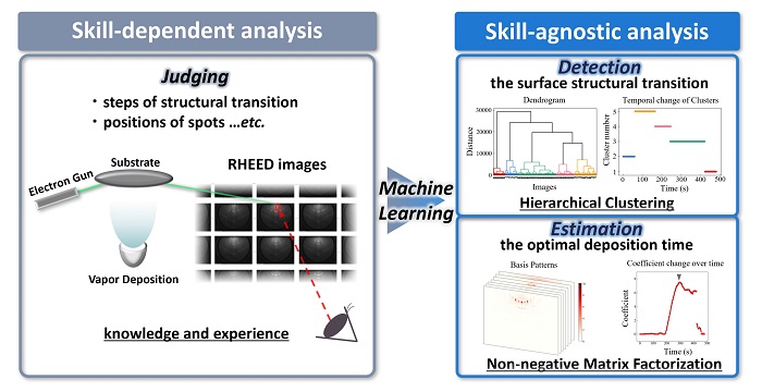
Unfortunately, for all its benefits, RHEED is sometimes hindered by the fact that its output patterns are complex and difficult to interpret. In virtually all cases, a highly skilled experimenter is needed to make sense of the huge amounts of data that RHEED can produce in the form of diffraction patterns. But what if we could make machine learning do most of the work when processing RHEED data?
A team of researchers led by Dr. Naoka Nagamura, a visiting associate professor at Tokyo University of Science (TUS) and a senior researcher at the National Institute for Materials Science (NIMS), Japan, has been working on just that. The team explored the possibility of using machine learning to automatically analyze RHEED data. This work, which was supported by JST-PRESTO and JST-CREST, was the result of joint research by TUS and NIMS, Japan. It was co-authored by Ms. Asako Yoshinari, Prof. Masato Kotsugi also from TUS, and Dr. Yuma Iwasaki from NIMS.
The researchers focused on the surface superstructures that form on the first atomic layers of clean single-crystal silicon (one of the most versatile semiconductor materials), depending on the number of indium atoms adsorbed and slight differences in temperature. Surface superstructures are atomic arrangements unique to crystal surfaces where atoms stabilize in different periodic patterns than those inside the bulk of the crystal, depending on differences in the surrounding environment. Because they often exhibit unique physical properties, surface superstructures are the focus of much interest in materials science.
First, the team used different hierarchical clustering methods, which are aimed at dividing samples into different clusters based on various measures of similarity. This approach serves to detect how many different surface superstructures are present. After trying different techniques, the researchers found that Ward’s method could best track the actual phase transitions in surface superstructures.
The scientists then sought to determine the optimal process conditions for synthesizing each of the identified surface superstructures. They focused on the indium deposition time for which each superstructure was most extensively formed. Principal component analysis and other typical methods for dimensionality reduction did not perform well. Fortunately, non-negative matrix factorization, a different clustering and dimensionality reduction technique, could accurately and automatically obtain the optimal deposition times for each superstructure. Excited about these results, Dr. Nagamura remarks that their “efforts will help automate the work that typically requires time-consuming manual analysis by specialists. We believe our study has the potential to change the way materials research is done and allow scientists to spend more time on creative pursuits.”
Overall, the findings reported in this study will hopefully lead to new and effective ways of using machine learning techniques for materials science—a central topic in the field of materials informatics. In turn, this would have implications in our everyday lives as existing devices and technologies are upgraded with better materials. “Our approach can be used to analyze the superstructures grown not only on thin-film silicon single-crystal surfaces, but also on metal crystal surfaces, sapphire, silicon carbide, gallium nitride, and various other important substrates. Thus, we expect our work to accelerate the research and development of next-generation semiconductors and high-speed communication devices,” concludes Dr. Nagamura.

