
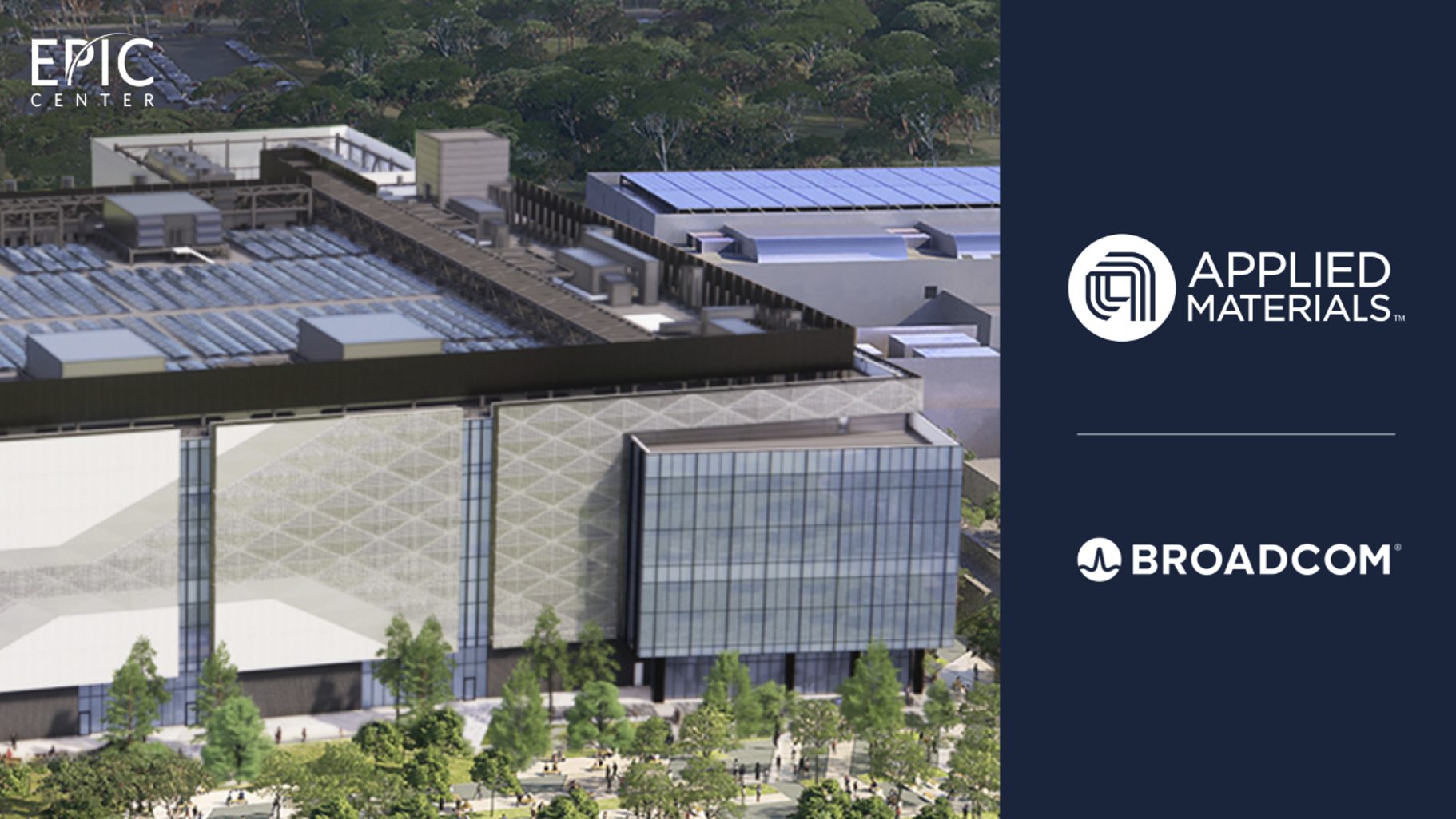
Companies to collaborate on R&D to accelerate the introduction of the latest packaging technologies for next-generation AI chips and systems. Partnership will leverage Applied’s global network of innovation centers, including the new EPIC Center in Silicon Valley.
Applied Materials, Inc., the leader in materials engineering for the semiconductor industry, today announces that Broadcom Inc. will join Applied’s EPIC platform as an innovation partner to accelerate the development of next-gen chip packaging technologies critical to next-generation AI systems.
The explosive growth of AI has driven a surge in demand for high-performance, energy-efficient compute infrastructure. To address this demand, chipmakers and system designers are increasingly adopting the latest packaging techniques and heterogeneous integration of multiple chips, aiming to boost energy-efficient performance across their systems. To unlock AI’s full potential, the industry is developing a new set of packaging building blocks to dramatically increase the interconnect density and bandwidth of tomorrow’s systems.




“The EPIC platform is designed to drive co-innovation across the ecosystem to change the way semiconductor technologies are developed and commercialized,” said Gary Dickerson, President and CEO of Applied Materials. “This new model gives leading system designers like Broadcom early access to foundational innovations in materials and process equipment, providing an opportunity for deep collaboration to accelerate the introduction of new advanced packaging technologies.”
“Close collaboration with partners throughout the supply chain is critical to delivering the next generation of high-performance AI systems,” said Charlie Kawwas, President of the Semiconductor Solutions Group at Broadcom. “By bringing together Applied’s expertise in materials engineering with Broadcom’s leading capabilities in semiconductor and system design, we can accelerate the time to market for innovations in AI.”
Through the EPIC platform partnership, Broadcom will leverage the R&D work taking place across Applied’s global innovation centers – driving progress in advanced packaging capabilities for connecting multiple chips within a computing system.
“Innovation in advanced packaging is essential to enabling sustainable progress in the AI era,” said Dr. Prabu Raja, President of the Semiconductor Products Group at Applied Materials. “We look forward to working side-by-side with Broadcom engineers to explore new technologies for boosting performance-per-watt through advanced chip packaging. With our global innovation platform and the new EPIC Center in Silicon Valley, Applied is uniquely positioned to help chipmakers and system designers accelerate the journey from concept to commercialization.”
“Cross-ecosystem collaboration has never been more important to address the rising complexity of chips for AI systems,” said Dilip Vijay, Vice President and Head of Global Operations for Silicon Products at Broadcom. “System designers must navigate a complex array of solution paths and packaging architectures, while simultaneously driving a faster cadence of product introductions. Collaborating with Applied will provide earlier access to the foundational technologies needed to accelerate progress in advanced packaging.”
Applied’s new EPIC (Equipment and Process Innovation and Commercialization) Center in Silicon Valley is the cornerstone of the company’s global EPIC platform. Representing the largest-ever U.S. investment in semiconductor equipment R&D, the center is designed from the ground up to dramatically reduce the time it takes to commercialize breakthrough technologies from early-stage research to full-scale manufacturing. The facility is on track to become operational in 2026.
Forward-Looking Statements
This press release contains forward-looking statements, including those regarding Applied’s investment and growth strategies, the development of new materials and technologies, industry outlook and technology requirements, the plans and expectations for the EPIC platform and Center, and other statements that are not historical facts. These statements and their underlying assumptions are subject to risks and uncertainties and are not guarantees of future performance. Factors that could cause actual results to differ materially from those shown by such statements include, without limitation: the demand for semiconductors and customers’ technology requirements; the ability to develop new and innovative technologies; the ability to obtain and protect intellectual property rights in key technologies; the ability to achieve the objectives of the EPIC platform and Center; and other risks and uncertainties described in Applied’s filings with the Securities and Exchange Commission, including Applied’s most recent Forms 10-K, 10-Q and 8-K. All forward-looking statements are based on management’s current estimates, projections, and assumptions, and Applied assumes no obligation to update them.
About Applied Materials
Applied Materials, Inc. is the leader in materials engineering solutions that are at the foundation of virtually every new semiconductor and advanced display in the world. The technology we create is essential to advancing AI and accelerating the commercialization of next-generation chips. At Applied, we push the boundaries of science and engineering to deliver material innovation that changes the world. Learn more at www.appliedmaterials.com.

