
– Anwesh Koley, Executive Editor, ELE Times
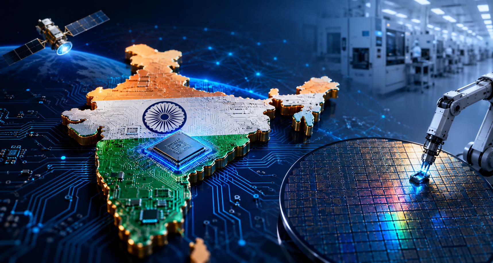
The government is serious about making India a global technology hub and how! After the visible success of the first phase of the India Semiconductor Mission, policy makers are walking the talk with the 2nd phase of the India Semiconductor Mission (ISM 2.0). In a move that could well be termed monumental, a staggering Rs 1,27,500 crore (around $13.25 billion) has been approved towards building an integrated semiconductor ecosystem across major Indian states.




The Indian semiconductor market is currently valued at around $45–$50 billion and is expected to expand to $100–$110 billion by 2030. At a time when India is working to strengthen its position in the global semiconductor supply chain, Semicon 2.0 is expected to provide a significant boost to India’s electronics and semiconductors industry. The emphasis of ISM 2.0 will be on deepening the country’s semiconductor and design ecosystem.
A Resilient Pursuit of Indigenous Capacity Expansion
What stands out is how Semicon 2.0 builds on the foundation laid by ISM 1.0. While the first phase focused on establishing India’s semiconductor base through ecosystem creation, ATMP/OSAT and early project execution, Semicon 2.0 is notably broader in scope – spanning chip design IP, equipment and materials, fabs, advanced packaging, R&D and talent development. While much of the conversation around chips has focused on fabrication plants, the latest developments indicate that India is building a broader ecosystem that includes packaging, testing, display manufacturing, and advanced materials.
Airing his views on phase 2 of the ISM, Amitesh Kumar Sinha, CEO, ISM, said, “As India’s semiconductor journey has already gathered momentum, the India Semiconductor Mission (ISM) has laid a strong foundation for semiconductor manufacturing in India, with 10 approved projects—including 2 fabs and 8 ATMP or OSAT units—attracting investments of around Rs 1.6 lakh crore. With ISM 2.0, the focus now shifts to deepening the value chain across materials, equipment, IP, and supply chain resilience.”
Harnessing Global Efficiencies
As India moves decisively from semiconductor policy to on-ground execution, ISM 2.0 provides a structured pathway to leverage the strengths of global partners in advanced manufacturing, supply chain integration, and design, while accelerating India’s capabilities across assembly, testing, packaging, the broader component ecosystem and overall Semiconductor ecosystem.
India sees strong potential for deeper participation from South Asian countries like Singapore across the value chain. “I would like to assure that ISM is all set to support any further investments in the sector. We are fully committed to facilitating and supporting such investments—ensuring a trusted, scalable, and globally competitive semiconductor ecosystem anchored in strong international partnerships,” affirmed Sinha.
As countries continue to diversify global chip supply chains, India’s semiconductor roadmap is increasingly viewed as a long-term manufacturing and strategic play rather than a short-term production target. India’s world-class engineering talent is a proven asset, and sustained R&D investments are expected to further elevate its position in the global supply chain.
What’s New in ISM 2.0
Finance Minister Nirmala Sitharaman announced ISM 2.0 in the Union Budget 2026, with an initial emphasis on design, equipment and materials. The announcement confirmed that Semicon 2.0 will broaden this framework further, encompassing design, machines and materials, fabs, the strengthening of ATMP/OSAT capabilities, research and development, and, significantly, talent development.
Indian Semiconductor Mission 1.0 focused on setting up basic chip making and packaging factories with a budget of Rs 76,000 crore. Taking this initiative a step further, Indian Semiconductor Mission 2.0 expands and strengthens the whole supply chain with a budget of Rs 1,27,500 crore. Indian Semiconductor Mission 1.0 made progress with 12 manufacturing units with investments over Rs 1.64 lakh crore. 24 Semiconductor design projects from startups have been approved for financial support while 105 startups have been granted access to EDA tools.
Under Indian Semiconductor Mission 2.0 government financial support is structured to deepen and strengthen the domestic value chain. For example, subsidies up to 40% on silicon fabrication plants and subsidies up to 35% on other fabrication plants. Semicon 2.0 is more diverse and deeper than ISM 1.0 because of the massive budget, focus on the semiconductor ecosystem, industry-led research and development centers and training programs, which lay the foundation for resilient supply chains and high value employment.
ISM 1.0 delivered approvals, investments, and early commercial production. Semicon 2.0 is aimed at deepening domestic capability across the value chain, from materials and equipment to advanced packaging, R&D, and skilled talent. If Semicon 1.0 was about proving that India can enter semiconductors, Semicon 2.0 is about proving that India can scale them.
The ISM (1.0 and 2.0) is critical for India Inc, because the growth of semiconductor supply and ecosystem is highly essential for India to build and grow its own microchip and semiconductor industry. This goes a long way in reducing foreign reliance, encouraging local and domestic industries, economic growth, employment, education, skill based teaching and national security. These foundational capabilities shield the country from global disruptions and foster sustainable, high value technical industries.
Key Components of Semicon 2.0
The Rs 1,27,500 crore initiative is a comprehensive push to build India’s semiconductor capabilities for the long term. Hailing this budgetary approval, Hitesh Garg, Vice President and India Managing Director, NXP Semiconductors, said, “As India progresses toward the vision of a “Viksit Bharat” by 2047, the Union Budget will be a critical lever in shaping the country’s medium- to long-term growth trajectory—particularly as global supply chains diversify and technology-led manufacturing becomes central to economic resilience and national competitiveness.”
Since ISM 1.0, the key focus has revolved around talent development, supply-chain readiness, access to raw materials, and long-term competitiveness against established semiconductor hubs. ISM 2.0 framework is expected to address some of these gaps by supporting equipment, chemicals, design ecosystems, and research capabilities. The key focus areas of Semiconductor 2.0 are broadly based on six pillars:
1) Design: The first pillar is based on chip design. Under phase 2, the aim is to develop designs of chips and systems and IPs. ISM 2.0 will focus on designing full stack Indian semiconductor intellectual property, and fortifying both domestic and global supply chains
2) Machines and Materials: Companies and Industries that are involved in the manufacturing process and research and development of machines, materials, chemicals that are essential for manufacturing semiconductors will be encouraged.
3) Setting up more fabrication plants: Efforts will be made to attract more manufacturers to come to India and set up fabrication plants to manufacture chips. Fabrication plants like silicon, compound semiconductor, display etc.
4) Strengthening the ATMP (Assembling, Testing, Marking and Packaging) industry: Setting up of ATMP/ OSAT units is encouraged for strengthening the semiconductor supply chain. Several approved proposals aim to leverage indigenous technologies for the assembly, testing, and packaging of semiconductor chips.
5) Research and Development: Research and Development of semiconductors is essential for advanced technological mechanisms to create better, faster electronic devices. The focus is on developing more advanced nodes and advanced technologies within and outside India.
6) Talent development: Talent development in semiconductors is the process of educating, training, and upskilling people to build a skilled workforce for chip design, manufacturing, testing, packaging, and research. With 315 universities training students using the latest EDA tools, about 68,000 students have already been trained.
“Government initiatives such as ISM 2.0 are a defining milestone in India’s journey toward global semiconductor leadership. By expanding support across the entire value chain from manufacturing and advanced packaging to critical materials and design, this initiative builds a foundation for long-term competitiveness,” Garg opined.
India Semiconductor Mission 2.0: Why it Stands Apart
By structuring Semicon 2.0 around six key pillars, the government has taken a holistic view of the industry. The clear roadmap that the sector’s future lays out is especially commendable. This is not merely about setting up a few fabs; it is about building the foundation for India’s semiconductor future over the coming years. While achieving this vision will require sustained effort, collaboration, investment, and strong industry-government partnership, the direction remains clear.
Airing his optimism for phase 2, Vinay Shenoy, MD, Infineon Technologies, India, said, “ISM 2.0 marks a decisive step in India’s journey from semiconductor consumer to semiconductor innovator. For Infineon, having invested in India’s ecosystem for over 25 years, this signals strong policy continuity and ambition. The enhanced focus reinforces our belief that India has the talent and capabilities to further strengthen its position as a global hub for chip innovation, particularly in areas driving decarbonization and digitalization.”
Policy Assurance
The government’s recent approvals, including projects in Gujarat, Odisha, Assam, and Uttar Pradesh, reflect a shift from policy announcements to infrastructure creation. Companies such as Tata Electronics, Micron, CG Power, and Kaynes Semicon are now part of a growing domestic semiconductor network that aims to reduce import dependence and strengthen India’s role in global electronics manufacturing.
NXP’s Garg further reiterated the semiconductor manufacturer’s commitment towards this massive capacity-building initiative. “At NXP, we are fully committed to this vision. We continue to advance cutting-edge R&D locally and nurture future-ready talent. We believe that collaborative ecosystem innovation is the key, and we look forward to partnering with industry, academia, and policymakers to drive India’s emergence as a global semiconductor hub.”
What makes this phase significant is the focus beyond just fabs. Advanced packaging technologies, display assembly, compound semiconductors, and supply-chain support systems are emerging as equally important areas. Industry observers believe this approach could help India gradually build capabilities in sectors linked to automotive electronics, telecom, AI hardware, and industrial devices.
Conclusion: A Robust Framework for India Semicon Inc
Through Semicon 2.0, India is demonstrating its readiness to emerge as a trusted and resilient partner in the global semiconductor value chain. The long-term policy support and substantial investment approved by the Cabinet underscore India’s determination to advance domestic capabilities and attract world-class semiconductor manufacturing to the country.
Semiconductor technology is at the heart of all critical technologies and India must catch up with the global leaders in this domain. Strategic strength and ability to lead development of new technologies, R&D and emerging areas of expertise cannot be achieved without electronics and semiconductors. ISM 2.0 is a timely move that will take us to the next level and deliver immense social and economic benefits for India.
This landmark announcement strengthens India’s backend semiconductor capabilities by enabling large-scale production of discrete chips tailored to high-growth sectors such as electric vehicles and industrial automation. Little wonder then, that as time progresses, India’s electronics and semiconductor ecosystem is steadily advancing towards becoming a self-reliant and globally competitive manufacturing hub.

