
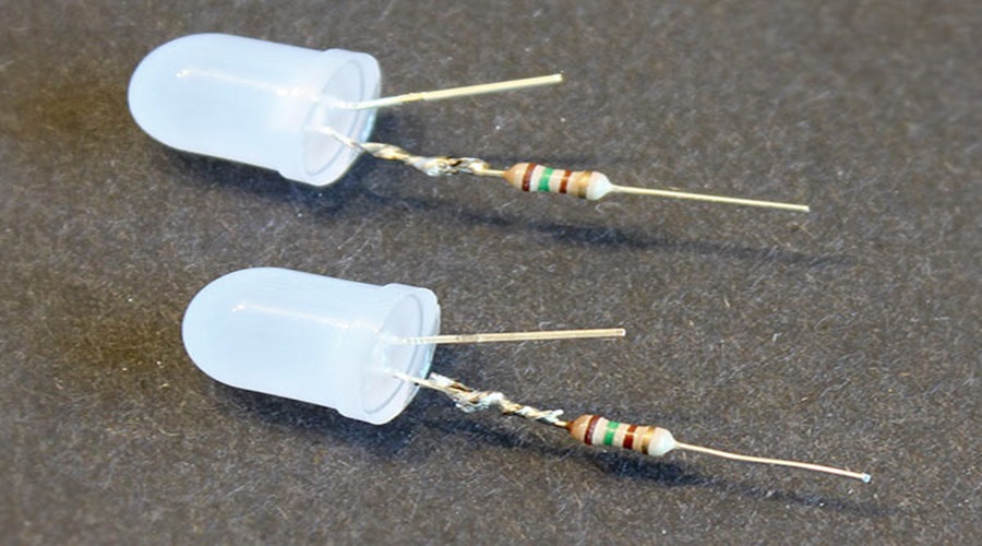
LED soldering is the process of joining electronic components of light-emitting diodes (LEDs) to a printed circuit board (PCB) or other substrates using a soldering material, typically a tin-lead alloy or lead-free solder. The process ensures proper electrical and mechanical connections between the LED terminals and the PCB.
How LED Soldering Works
- Preparation:
- Ensure that the PCB and LED components are clean and free from debris or oxidation.
- Apply solder paste to the PCB pads where the LED will be placed.
- Placement:
- Position the LED on the solder-pasted area using precision tools like tweezers or pick-and-place machines.
- Soldering Process:
- Hand Soldering:
- Use a soldering iron to heat the LED terminals and solder pads.
- Apply solder wire to create a strong electrical connection.
- Reflow Soldering (for mass production):
- The PCB with the LED is placed in a reflow oven, where heat melts the solder paste, creating a secure connection.
- Wave Soldering:
- For through-hole LEDs, the PCB is passed over a molten solder wave to attach the components.
- Hand Soldering:
- Inspection:
- Verify the connections using visual inspection, automated optical inspection (AOI), or X-ray inspection.
- Testing:
- Test the soldered LED for functionality, ensuring it emits light and operates as intended.
LED Soldering Process
- Manual Soldering:
- Used for prototypes or small batches.
- Involves a soldering iron and manual placement.
- Automated Soldering:
- Uses pick-and-place machines and reflow ovens for large-scale production.
- Soldering Techniques:
- Surface-Mount Technology (SMT): Common for LEDs mounted on flat PCBs.
- Through-Hole Technology (THT): Used for LEDs requiring a stronger mechanical bond.
- Cooling:
- Allow the soldered assembly to cool, solidifying the solder joints.
Uses & Applications of LED Soldering
- Consumer Electronics:
- LED displays, backlights, and indicators in devices.
- Automotive:
- Headlights, tail lights, and dashboard indicators.
- Industrial:
- Machine vision lighting and control panels.
- Residential and Commercial Lighting:
- LED bulbs, tube lights, and architectural lighting.
- Signage and Displays:
- Advertising boards, billboards, and traffic signals.
Advantages of LED Soldering
- Durability:
- Provides a robust mechanical and electrical connection.
- Scalability:
- Suitable for mass production using automated techniques.
- Efficiency:
- Reflow soldering ensures uniform heat distribution and reliable connections.
- Versatility:
- Applicable to various LED sizes and designs.
- Energy Efficiency:
- LED soldering supports energy-efficient lighting technologies.
Disadvantages of LED Soldering
- Heat Sensitivity:
- LEDs are sensitive to high temperatures, which can damage components if not controlled.
- Complexity:
- Requires precision in placement and temperature control during soldering.
- Material Costs:
- Lead-free solders and automated equipment can increase production costs.
- Risk of Cold Solder Joints:
- Improper soldering can result in weak or intermittent connections.
- Environmental Concerns:
- Lead-based solder can pose environmental and health risks if not disposed of properly.




