

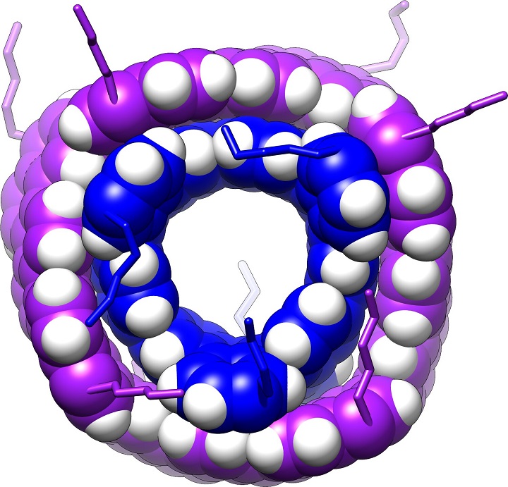
Material behaviours depend on factors including the composition of the material and the arrangement of its molecular parts. For the first time, researchers have found a way to coax Carbon Nanotubes into creating moiré patterns. Such structures could be useful in materials research, particularly in the field of superconducting materials.
Professor Hiroyuki Isobe from the Department of Chemistry at the University of Tokyo and his team create Nanoscopic material structures, primarily from carbon. Their aim is to explore new ways to create carbon nanostructures and to find useful applications for them. The most recent breakthrough from their lab is a new form of Carbon Nanotube with a specific arrangement of atoms.



“We successfully created different kinds of atom-thick Carbon Nanotubes which self-assemble into complex structures,” said Isobe. “These nanotubes are made from rolled-up sheets of carbon atoms arranged hexagonally. We made wide ones and narrow ones which fit inside them.
This means the resulting complex tube structure has a double-layered wall. The hexagonal patterns of these layers are offset such that the two layers together create what is known as a moiré pattern. And this is significant for materials researchers.”
When repeating patterns overlay one another, a new resultant pattern emerges. If you then move one of the layers, or if you move relative to the layers, the resultant pattern will change slightly, for example, if you look at a screen door through a mesh curtain, or if you hold two sieves together.
The team’s moiré patterns emerge when one hexagonal grid of carbon atoms is rotated slightly relative to another similar hexagonal grid.
These patterns aren’t just for show; they can imbue materials with functional properties. Two areas that might especially benefit from the properties created here are synthetic chemistry, as the moiré carbon bilayer tubes could be challenging yet attractive targets of molecular self-assembly, and superconducting materials, which could lead to a generational leap in electrical devices that require far less power to run and would be far more capable than current devices.

