
Lifetime Analysis
Current lifetime models for power modules employing standard technologies underline the impact of the temperature difference ΔT, the mean or maximum junction temperatures Tvjm, Tvjmax and the duration of the load current ton during one cycle on the estimated lifetime of a power module. Even though these models are empirical, ΔT, Tjm and ton can be related to driving forces of degradation. The first lifetime model presented was later extended by adding terms that describe the impact of ton, the current per bond-foot, the voltage class U, with respect to chip thickness, and the bond-wire diameter D.
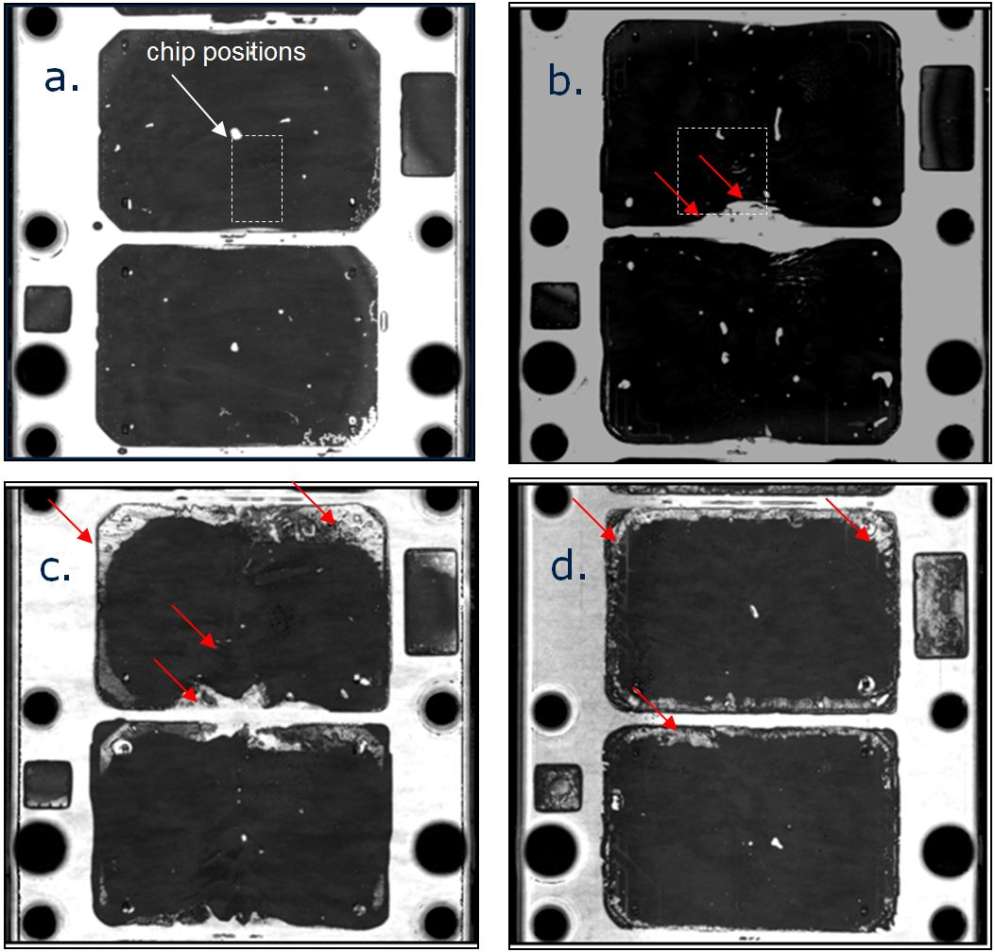
a) After 150.000 active cycles @ ΔT≈108 °C and ton = 2 s.
b) After 125.000 active cycles @ ΔT≈120 °C and ton = 5 s.
c) After 66.000 active cycles @ ΔT≈140 °C and ton = 60 s.
d) After 3000 passive thermo-shock cycles from -40 °C to 150 °C


For the development of a first lifetime model focusing on the new die attach technologies, the power cycling results presented were revised. Most importantly, failure data from samples with different die attach technologies were grouped together. This is a valid approach since the failure is always related to the substrate-to-baseplate solder.
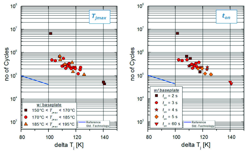
Figure 3 presents the excellent power cycling results of PrimePACK modules employing .XT with regard to Tvjmax and ton. For comparison, the results of standard technology are added to the graph.
The examination of the copper wire bond connection out of this PC test does not reveal degradation. Thereby it can be concluded that bond failure will not be an issue for the new joint technology .XT.
The degradation pattern in the baseplate solder can be analyzed by means of scanning acoustic microscopy (SAM). Figure 4 depicts the results and underlines the impact of ton. For ton=2 s, the degradation of the solder starts directly below the chip (Figure 4 a). Increasing ton from 2 to 5 s leads to a higher ΔT at the edges of the substrate-to-baseplate solder joint which in turn manifests itself in additional shear forces and a more dominant degradation at the edges compared to the beginning of the test (Figure 4 b). It has to be underlined, that the sample from Figure 4a afterwards reached more than 6∙106 cycles.
When ton is increased even further to 60 s, this effect becomes even more apparent as degradation is strongly accelerated at the edges of the baseplate-solder (Figure 4c). For this load, the degradation pattern bears strong resemblance to that obtained after passive thermal cycling. With the findings from it can be expected that a further increase of ton would lead to a complete shift of the critical degradation from below the chip to the edges of the DCB.
On the other hand, a further reduction of ton is expected to result in significantly higher lifetime – independent from ΔT – as the stress in the substrate-to-baseplate solder is reduced significantly.
Summary
In contrast to standard joining technology, the wire-bond related failure loses importance as bond failure can be excluded with .XT. By increasing ton, the degradation of the baseplate solders joint shifts from below the chips toward the substrate´s edges and becomes the most prominent EOL mechanism. The .XT lifetime is still dependent on Tvjmax and ton but is shifted to much higher numbers of cycling.
Based on this and in comparison to EOL mechanism of standard joining technologies, aluminum wire-bond and soft-soldering die attach, the .XT joining technology provides a major advantage with respect to lifetime. The described results of the lifetime research will be implemented in new lifetime models of the innovative .XT interconnect technologies.