HomeTechnologyCooking up Next-gen Semiconductors

    Cooking up Next-gen Semiconductors

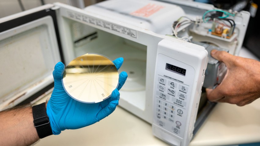
    A household microwave oven modified by a Cornell engineering professor is helping to cook up the next generation of cellphones, computers, and other electronics after the invention was shown to overcome a major challenge faced by the semiconductors industry.

    As microchips continue to shrink, silicon must be doped, or mixed, with higher concentrations of phosphorus to produce the desired current. Semiconductor manufacturers are now approaching a critical limit in which heating the highly doped materials using traditional methods no longer produces consistently functional semiconductors.

    The Taiwan Semiconductor Manufacturing Company (TSMC) theorized that microwaves could be used to activate the excess dopants, but just like with household microwave ovens that sometimes heat food unevenly, previous microwave annealers produced “standing waves” that prevented consistent dopant activation.

    TSMC partnered with Hwang, who modified a microwave oven to selectively control where the standing waves occur. Such precision allows for the proper activation of the dopants without excessive heating or damage to the silicon crystal.

    This discovery could be used to produce semiconductor materials and electronics appearing around the year 2025, said Hwang, who has filed two patents for the prototype.

    “A few manufacturers are currently producing semiconductor materials that are 3 nanometers,” Hwang said. “This new microwave approach can potentially enable leading manufacturers such as TSMC and Samsung to scale down to just 2 nanometers.”

    The breakthrough could change the geometry of transistors used in microchips. For more than 20 years, transistors have been made to stand up like dorsal fins so that more can be packed on each microchip, but manufacturers have recently begun to experiment with a new architecture in which transistors are stacked horizontally. The excessively doped materials enabled by microwave annealing would be key to the new architecture.

    ELE Times Research Desk
    ELE Times Research Deskhttps://www.eletimes.ai
    ELE Times provides extensive global coverage of Electronics, Technology and the Market. In addition to providing in-depth articles, ELE Times attracts the industry’s largest, qualified and highly engaged audiences, who appreciate our timely, relevant content and popular formats. ELE Times helps you build experience, drive traffic, communicate your contributions to the right audience, generate leads and market your products favourably.

    Related News

    Must Read

    Building Reliable 5G and 6G Networks Through Mobile Network Testing

    The development of communication networks has entered a revolutionary...

    Beyond the Screen: envisioning a giant leap forward for smartphones from physical objects to immersive experiences

    Author: STMicroelectronics Smartphones have become some of the most ubiquitous...

    Microchip’s SkyWire Tech Enables Nanosecond-Level Clock Sync Across Locations

    To protect critical infrastructure systems, SkyWire technology enables highly...

    Next Generation Hybrid Systems Transforming Vehicles

    The global automotive industry is undergoing a fundamental transformation...

    Tobii and STMicroelectronics enter mass production of breakthrough interior sensing technology

    Tobii and STMicroelectronics announced the beginning of mass production...

    Rohde & Schwarz unveils compact MXO 3 oscilloscopes with 4 and 8 channels

    Rohde & Schwarz expands its next-generation MXO oscilloscope portfolio...

    TI’s new power-management solutions enable scalable AI infrastructures

    Texas Instruments (TI) debuted new design resources and power-management...

    ESA awards Rohde & Schwarz for contributions to 30 years European Satellite Navigation

    The event brought together institutional and industrial partners, ESA...