
Courtesy: Lam Research
| ● Controlling critical process parameters is key to managing edge placement error (EPE)
● Simulations revealed that only 9.75% of runs met the minimum line CD success criteria |
As the complementary metal-oxide semiconductor (CMOS) area shrinks 50% from one node to the next, interconnect critical dimensions (CD) and pitch (or spacing) are under tight demands.


At the N3 node, where metal pitch dimensions must be at or below 18 nm,1,2 one of main interconnect challenges is securing sufficient process margins for CD and edge placement error (EPE).
- Achieving the CD gratings for future technology nodes requires multi-patterning approaches, such as self-aligned double/quadruple/octuple patterning (SADP/SAQP/SAOP) and multiple litho-etch (LE) patterning, combined with 193i lithography or even EUV lithography.
SEMulator3D virtual fabrication, part of Semiverse Solutions, was used in a Design of Experiments (DOE) to evaluate EPE and demonstrate the ability to successfully pattern an advanced 18- and 16-nm metal pitch (MP) BEOL.
Using a process model, we explored the impact of process variations and patterning sensitivities on EPE variability. The simulation identified significant process parameters and corresponding process windows that need to be controlled for successful EPE control.
Simulation of 18-nm BEOL Process
A self-aligned litho-etch litho-etch (SALELE) scheme with self-aligned blocks was proposed for an 18-nm MP BEOL process flow used at the N3 node. The advantage of this scheme is that no dummy metal is used in the BEOL, which helps reduce parasitic capacitance.
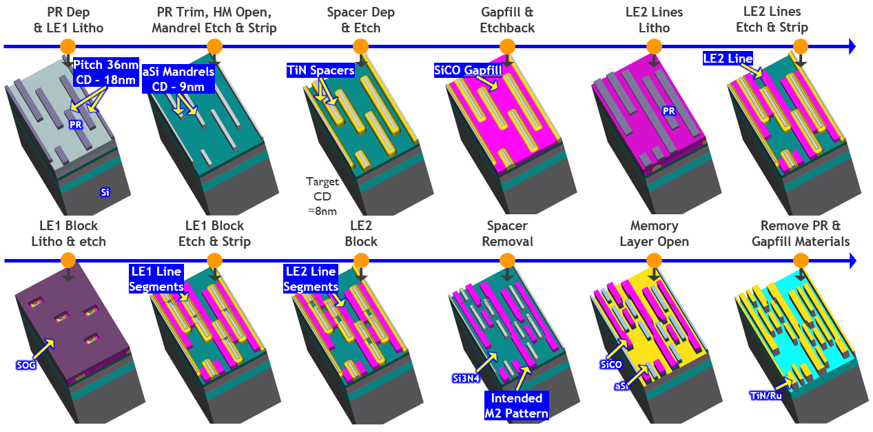
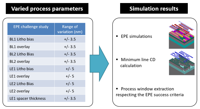
Figure 2 highlights the selected process parameters and corresponding range values used in the DOE simulation. Multiple process parameters that could affect the dimensions of the lines and blocks were varied during simulation using a uniform Monte Carlo distribution.
Parameters such as BL1 Litho bias and LE2 overlay, with range of variation. Simulation results included EPE simulations and Minimum line CD calculation.
In this study, three challenging EPE measurements were evaluated:
- EPE1: EPE calculation of the gap between the printed silicon mandrels for litho etch 1 (LE1) and printed silicon oxycarbide lines for litho etch 2 (LE2)
- EPE2: EPE calculation of the gap between the printed BL1 (block 1) mask after BL1 etch and printed LE1 lines
- EPE3: EPE calculation of the gap between the printed BL2 (block 2) mask after BL2 etch and the printed LE2 lines
Monte Carlo simulations were performed in SEMulator3D across 800 runs using a uniform distribution. For each simulation event, the EPE was extracted using virtual measurements. Process sensitivity analysis was performed in the simulation to investigate the impact of process variations (Figure 2) on the EPE challenges.
The most important process parameters that could impact line dimensions and EPE were automatically identified using the SEMulator3D® Analytics module. Process sensitivity analysis was performed to explore the impact of the most significant parameters on each EPE challenge.
DOE Results
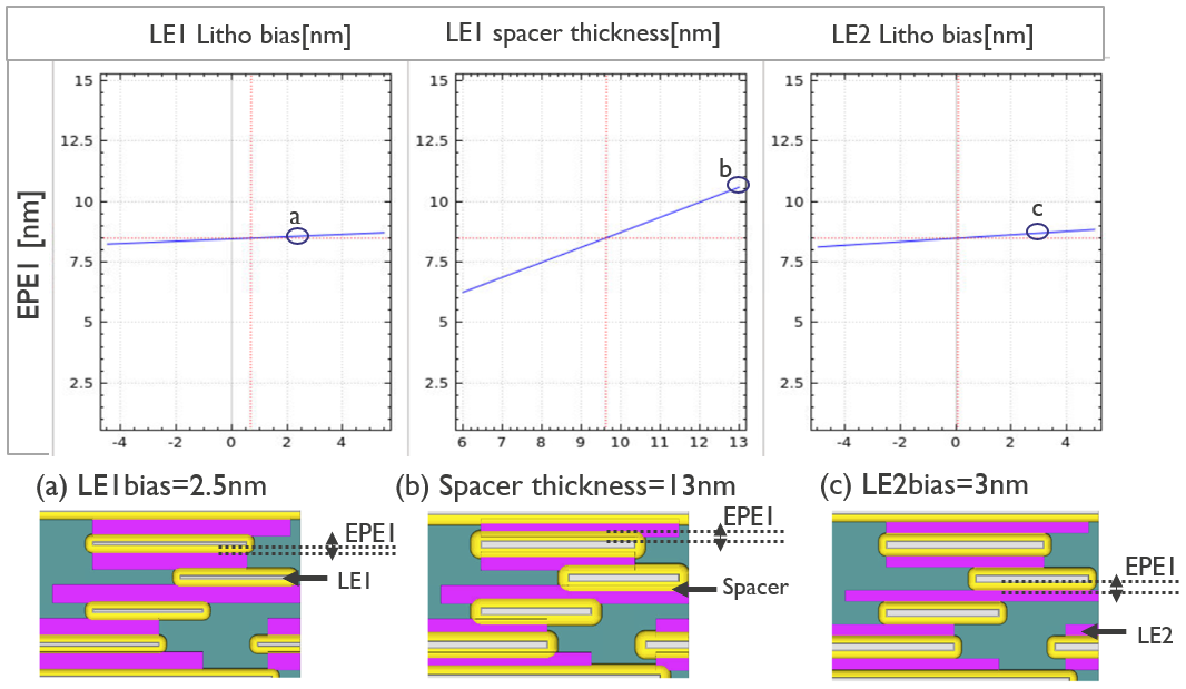
Figure 3 displays an EPE sensitivity analysis plot of EPE1: LE2 on LE1. Spacer thickness defines the gap between the LE2 and LE1 line segments. EPE1 is significantly dependent on spacer thickness variation and less sensitive to LE1 and LE2 litho bias variations.
Three graphs and corresponding virtual representations:-
The same EPE sensitivity analysis methodology used in Figure 3 was applied to EPE2 and EPE3. The process sensitivity analysis plots of EPE allowed us to identify acceptable process windows for all three (EPE1, EPE2, and EPE3).
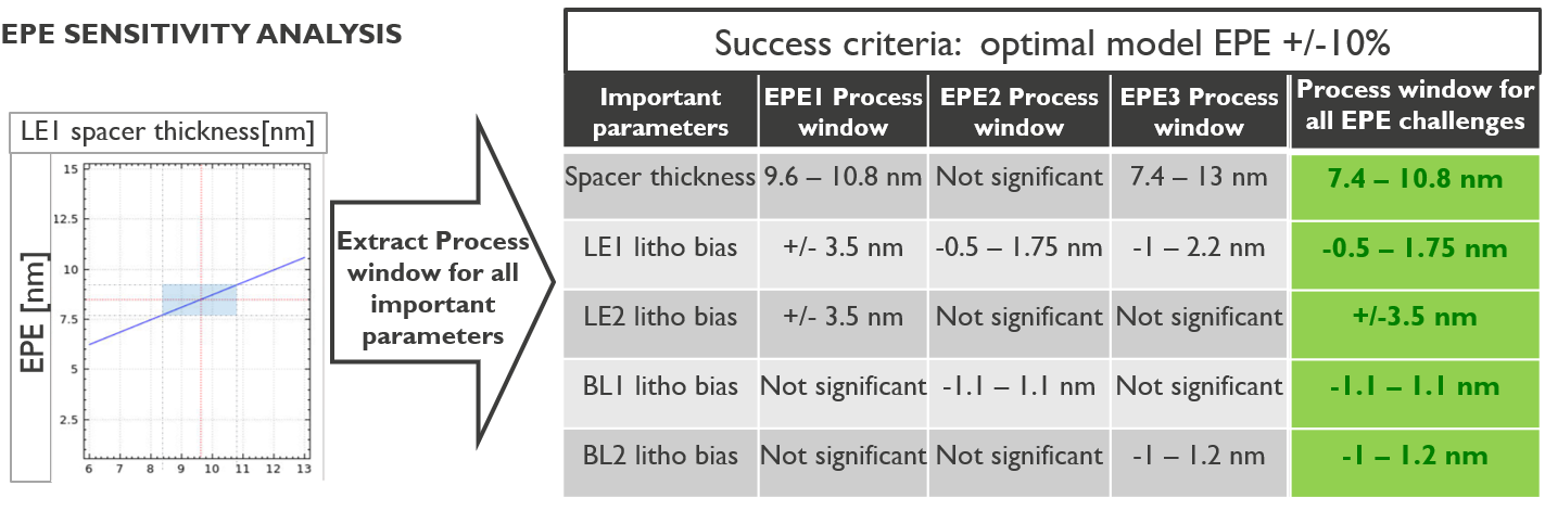
Figure 4 summarizes EPE process windows that were extracted from our process model for the significant process parameters identified earlier.
EPE sensitivity analysis with the extracted process window for all important parameters such as spacer thickness, LE1 litho bias, and BL1 litho bias
Along with evaluating process windows needed to avoid the EPE challenges, minimum line CD was virtually measured for each simulated run. Figure 5 depicts the minimum line CD process window needed to meet the line CD success criteria (8nm<CD<10nm).
Our simulation results indicated that only 9.75% of runs displayed a minimum line CD between 8 and 10 nm. Thus, in addition to the EPE challenge, minimum line CD control is critical and should be considered as part of the process window definition.
Dots on a graph showing a concentration of runs below 10 nm for minimum CD
This study demonstrates that virtual fabrication is a powerful tool for identifying process windows and margins essential for next-generation interconnect technologies. By simulating and analyzing critical process parameters, engineers can proactively address yield-limiting failures and optimize both minimum line CD and EPE control. These insights are vital for advancing semiconductor manufacturing at the 3-nm node and beyond.