
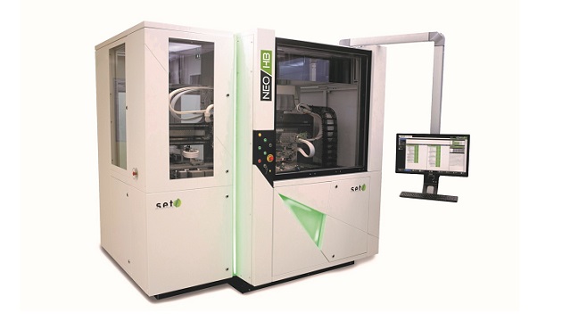
SET, Smart Equipment Technology, the leading supplier in high accuracy die-to-die and die-to-wafer bonders, announced the release of NEO HB, an automatic flip-chip bonder designed for ± 1 µm 3σ post-bonding accuracy, in stand-alone or full automatic mode (EFEM). NEO HB is suitable for direct hybrid bonding processes.
The first of a new line of SET flip-chip bonders dedicated entirely to production, the tool combines high precision, flexibility, short cycle time, and creative design. It was developed in collaboration with CEA-Leti as part of IRT Nanoelec’s 3D integration program.




“SET joined IRT Nanoelec in 2016 with the goal to develop a brand-new tool for direct-bonding applications that delivered high accuracy and high throughput, and a high level of cleanliness,” said Pascal Metzger, CEO of SET. “That ambition required a strong collaboration among experts from different disciplines. Today, SET’s team is proud to commercially launch NEO HB, which meets the initial technical targets and will address development and production needs for tomorrow’s chips.”
“This intensive, exciting, and fruitful collaboration allowed us to design a bonding solution adapted to fine-pitch assembly needs,” added Nicolas Raynaud, project manager at SET.
Séverine Chéramy, director of IRT Nanoelec’s 3D integration program, said the objective when SET joined the consortium was to provide IC designers with 3D die-to-wafer stacking at an aggressive pitch – less than 10µm – at high speed, at room temperature, and without pressure or underfill.
“Achieving this goal with NEO HB is a major success of the 3D program and highlights the IP and expertise offered by IRT Nanoelec,” she said. “By overcoming daunting technical challenges and building this bonder, the team has opened the huge potential of die-to-wafer direct hybrid bonding technologies for a wide range of applications.”
Hughes Metras, the recently appointed director of Nanoelec, said the institute’s collaboration with SET demonstrates both the success of its mission of technology development and transfer and the strength of its 3D integration program.
“For the past eight years, I was strongly engaged in the promotion of 3D technologies developed within our IRT and I believe this achievement outlines the added value of our institute for the local ecosystem in advanced semiconductor technologies,” Metras said.
For more information, visit: www.irtnanoelec.fr and www.set-sas.fr/en/

