

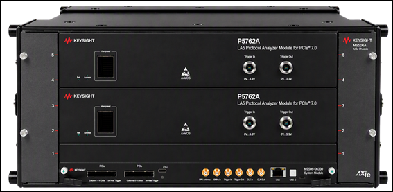
Keysight Technologies, Inc. today introduced its Protocol Test Solution for PCIe 7.0, an integrated platform that enables engineers to bring up, validate, debug, and verify compliance of next-generation devices and systems at the protocol layer. By combining instant link-up with deep visibility at 128 GT/s, the solution helps development teams identify issues earlier, reduce validation risk, and accelerate the delivery of next generation high-speed PCIe interconnect required for artificial intelligence and data centre infrastructure.
As artificial intelligence workloads increase demand for compute and data bandwidth, PCI Express 7.0 provides next generation interconnect performance by doubling the raw data rate to 128 GT/s. PCI Express 7.0 is expected to become the dominate interconnect for rack-scale systems connecting graphics processing units, accelerators, switches, memory, and storage. This performance increase makes link establishment, protocol behaviour, and interoperability more difficult to validate across increasingly complex architectures.



Reliable link-up is the foundation for meaningful protocol analysis. At the fastest PCIe speeds, engineers need immediate visibility to investigate link training and status state machine (LTSSM) behaviour, FLIT-based encoding, protocol errors, and complex transaction layer issues to isolate problems before they lead to redesigns or cause schedule delays. Keysight addresses this challenge with an architecture designed to provide stable and reliable analysis without analyser tuning, helping teams move from connection to actionable insight faster.
The solution combines a full-featured protocol analyser and exerciser, test platform, and dedicated analysis software. The integrated workflow offers early adopters both a link partner for device bring-up and extensive protocol visibility needed to progress from initial silicon validation through interoperability and compliance testing.
Key benefits of the Protocol Test Solution for PCIe 7.0 include:
- Accelerates time to first measurement: Advanced signal integrity enables reliable protocol trace capture without analyser tuning, giving engineers repeatable results and faster insight.
- Identifies protocol issues faster: Deep visibility into LTSSM transitions, FLIT-based encoding, protocol errors, and transaction layer packet transactions help teams accelerate debug, isolate root causes, validate reliable operation, and verify compliance to PCI Express specifications.
- Reduces early silicon risk: Early collaboration and test availability help teams uncover protocol and interoperability issues sooner, minimizing late-stage rework and shortening development cycles.
- Streamlines end-to-end validation: An integrated analyser, exerciser, test platform, and software environment provides a consistent workflow from bring-up through validation and compliance testing.
- Advances AI infrastructure development: Support for rack-level interconnects and backward compatibility helps engineers validate next-generation scale-up architectures while protecting existing test investments and easing migration.
Neeraj Paliwal, Senior Vice President, Silicon IP Product Management, Synopsys, said: “Establishing a reliable PCIe 7.0 link at 128 GT/s between production silicon and protocol test equipment is a key interoperability milestone. Validating our silicon-proven Synopsys PCIe 7.0 IP solution with Keysight’s protocol solution means customers can commit to their next-generation AI and data centre designs with confidence.”
Dr. Joachim Peerlings, Vice President of Network and Data Center Solutions, Keysight, said: “Successful PCIe 7.0 deployment depends on proven ecosystem interoperability alongside bandwidth advancements. Our collaboration with Synopsys helps customers validate designs earlier, identify issues faster, and gain confidence in the readiness of next generation silicon and systems. Together, we’re accelerating the path from innovation to deployment for AI and data centre applications.”

