
Water is the secret ingredient in a simple way to create key components for solar cells, X-ray detectors, and other optoelectronics devices.
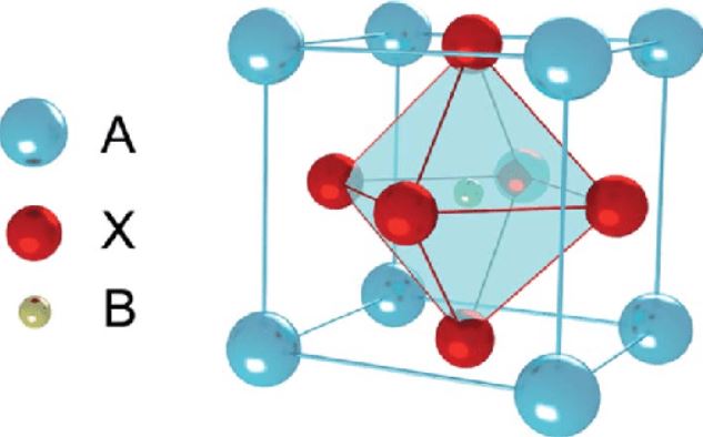
The next generation of photovoltaics, semiconductors, and LEDs could be made using perovskites—an exciting and versatile nanomaterial with a crystal structure.


Perovskites have already shown similar efficiency to silicon, are cheaper to make, and feature a tunable bandgap, meaning the energy they are able to absorb, reflect or conduct can be changed to suit different purposes.
Ordinarily, water is kept as far away as possible during the process of creating perovskites. The presence of moisture can lead to defects in the materials, causing them to fall apart more quickly when they’re being used in a device.
That’s why perovskites for scientific research are often made via spin coating in the sealed environment of a nitrogen glove box.
Now, though, members of the ARC Centre of Excellence in Exciton Science have found a simple way to control the growth of phase-pure perovskite crystals by harnessing water as a positive factor. This liquid-based mechanism works at room temperature, so the approach remains cost-effective.
Led by researchers at Monash University, the team found that by changing the ratio of water to solvent during the early stages of the process, they could choose to grow different types of perovskite crystals, with structures to suit various purposes.
Corresponding author Dr. Wenxin Mao of Monash University said: “By carefully tuning the concentration of water in the precursor solution, we realized the precise control of particular perovskite phases.”
Computational and thermodynamic analysis conducted by colleagues at the University of Sydney identified that the coordination of lead and bromide ions in the precursor solution was an important factor in determining which types of crystals are formed.
Lead author Qingdong Lin, a Ph.D. student at Monash University, said: “We now understand the internal mechanics and function of water inside the precursor solution. By doing that we can further use water to control the crystallization process.”
To demonstrate the quality of the end product, crystals produced via this approach were coupled with back-contact electrodes through nanofabrication to create X-ray detection devices.
This test sample performed at a similar level to commercial X-ray detectors currently being used in real-world settings, like medical imaging and Geiger counters, and out-performed prototype perovskite X-ray detectors developed using slower, more complicated fabrication methods.
Wenxin said: “We compared them with commercial X-ray detectors as well as other types of perovskites and we do have a very good responsivity and sensitivity to X-rays. Overall this project shows that we have found a smart way to control inorganic perovskite single crystals.
“The methodology is flexible and feasible and doesn’t require a very unique environment or technique to apply it.”
As well as solar cells, X-ray detectors, and LEDs, perovskites created with this method could also be useful in UV light detection, lasers, and solar concentrators.