
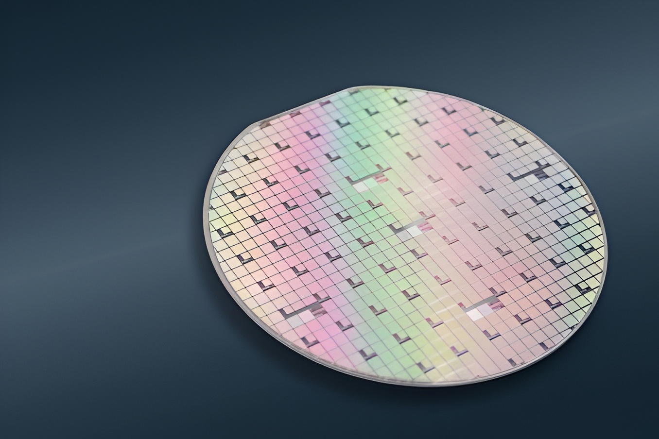
Semiconductor manufacturer onsemi, specialised in silicon carbide (SiC) power solutions, power management, and CMOS image sensors has introduced its Embedded Power Platform—a wafer-level power architecture that integrates multiple dies (silicon, SiC, and GaN) directly into a single system. This new semiconductor packaging architecture enables higher power density, lower electrical losses and easier power-system integration. This platform has the potential to develop traction inverters and power systems that are smaller and more efficient for EVs.
onsemi announced the Embedded Power Platform on September 16, 2026, at its headquarters in Scottsdale, Arizona, USA. The architecture delivers up to 3-5 times higher power density compared to current traction inverters. It supports the integration of silicon, silicon carbide, and gallium nitride (GaN) technologies, along with field-effect transistors, drivers, and controllers.




Advance Packaging Reduces EV Power Losses
Traction Inverter design developed by onsemi replaces high-inductive wire bonds with precision wafer-level redistribution layers (RDLs). This method reduces inductance and performs higher switching frequency operations. It reduces heat loss and increases EV traction inverter efficiency by addressing both thermal and performance challenges simultaneously.
Subaru Corporation, a Japanese multinational automotive manufacturing company has shown interest in implementing this embedded power platform developed by onsemi in its future electrified vehicles. This technology engagements between industries allows them to explore methods that can enhance energy efficiency, reduce development complexity, and facilitate next-generation vehicle architecture.

