
In simulations and experiments, researchers demonstrate that introducing tiny nanoscale texturing on the surfaces of materials in perovskite/silicon tandem solar cells can significantly increase efficiency by reducing the amount of light energy that is lost due to reflection. A new nanotextured design can achieve a power conversion efficiency potential above 29%, which simulations suggest could be further improved with better fabrication techniques and additional texturing.
Philipp Tockhorn from Helmholtz-Zentrum Berlin (HZB) will present the work at the virtual OSA Advanced Photonics Congress to be held is scheduled for 29 July.


“We present nanotextured perovskite/silicon tandem solar cells that are on par with the best cells presented in this highly dynamic field,” said Tockhorn. Our findings may contribute to the further development of highly efficient perovskite/silicon tandem solar cells and have the potential to further decrease the cost of solar electricity.”
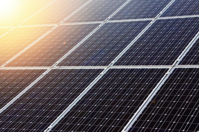
Perovskites are materials with a crystal structure similar to that of the naturally-occurring mineral perovskite. These semiconducting materials convert sunlight to energy very efficiently and have been a key focus for the development of next-generation solar energy technologies. Today’s solar panels are made primarily from silicon.
For the new work, Tockhorn, Johannes Sutter and colleagues from the groups of Prof. Becker and Prof. Albrecht at HZB examined how introducing nanotexturing at various interfaces affects the performance of tandem solar cells made from a perovskite solar cell atop a silicon solar cell. They first used a computer simulation to calculate the electric current in the perovskite and silicon subcells (the photocurrent density) when the perovskite layer was totally flat, nanotextured (bumpy) only on the bottom where it met the silicon layer, or bumpy on both top and bottom. The simulated bumps were about 300 nm high and 750 nm apart. While the one-sided nanotextured design showed only slight performance improvement over the flat design in the simulation, the fully textured architecture was calculated to absorb considerably more light, increasing the photocurrent density by 0.7 mA/cm2 per subcell.
To further explore how nanotexturing affects solar cell performance, the researchers then fabricated different perovskite/silicon tandem solar cell designs: one with a fully flat perovskite layer and one with a perovskite layer that is flat on top and bumpy on the bottom at the interface to the silicon solar cell. They determined that the one-sided nanotexturing already increased the light absorbed and current generated in the silicon absorber layer by 0.2-0.3 mA/cm².
“Remarkably, the nanotextures not only improve the light absorption but also lead to a slight enhancement of the tandem solar cell’s electronic quality in comparison to the planar reference in conjunction to better film processing conditions, Tockhorn said.”
The findings suggest a promising avenue for further improvements, according to the HZB researchers. Based on their simulation results, the researchers predict that a solar cell where the perovskite layer is nanotextured on both top and bottom would likely further increase performance and reach power conversion efficiency exceeding 30%.
“A further development of this double-sided textured approach is existing and feasible but will require improvements in the fabrication process to add nanotexturing to the top side of the perovskite layer,” Tockhorn said.