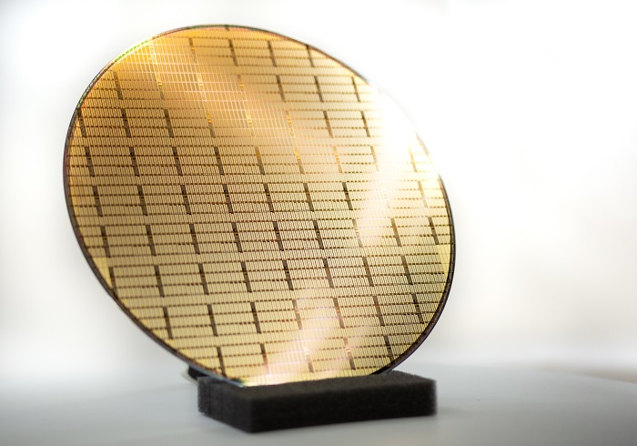
Infineon Technologies AG and Panasonic Corporation have signed an agreement for the joint development and production of the second generation (Gen2) of their proven gallium nitride (GaN) technology, offering higher efficiency and power density levels. The outstanding performance and reliability combined with the capability of 8-inch GaN-on-Si wafer production mark Infineon’s strategic outreach to the growing demand for GaN power semiconductors. In accordance with market requirements, Gen2 will be developed as 650 V GaN HEMT. The devices will allow for ease of use and provide an improved price-performance ratio, targeting, amongst others, high- and low-power SMPS applications, renewables, motor drive applications.
For many designs, gallium nitride (GaN) offers fundamental advantages over silicon. The outstanding specific dynamic on-state resistance and smaller capacitances compared to silicon MOSFETs qualify GaN HEMTs for high-speed switching. The resulting power savings and total system cost reduction, operation at higher frequencies, improved power density, and overall system efficiency make GaN a very attractive choice for design engineers.
“In addition to the same high reliability standards as for Gen 1, with the next generation customers will benefit from even easier control of the transistor as well as a significantly improved cost position, thanks to moving to an 8-inch wafer manufacturing,” says Andreas Urschitz, President of Infineon’s Power and Sensor Systems Division. Like the jointly developed Gen 1 devices, known as Infineon’s CoolGaN and Panasonic’s X-GaN™, the second generation will be based on the normally-off GaN-on-silicon transistor structure. This, in combination with the unmatched robustness of the hybrid-drain-embedded gate injection transistor (HD-GIT) structure, makes these components the product of choice and one of the most long-term reliable solutions in the market.
“We are delighted to extend our partnership and collaboration with Infineon on GaN components. Within the joint approach, we will be able to apply Gen1 and Gen2 devices on high quality and based on latest innovation developments”, says Tetsuzo Ueda, Associate Director of Engineering Division, Industrial Solutions Company, Panasonic Corporation.
For more information, visit www.infineon.com


