
Courtesy: Lam Research
- As advanced logic chips decrease in size, voltage loss can increase
- An emerging solution is backside power delivery networks that use SABC architecture
The problem: As metal pitch scaling shrinks to support the next generation of logic devices, the IR (or voltage) drop from conventional frontside connections has become a major challenge.


As electricity travels through a chip’s metal wiring, some voltage gets lost because wires have resistance.
- If the voltage drops too much, the chip’s transistors can’t get enough power and can slow down or fail.
- In addition, the resistance of back-end-of-line (BEOL) metal lines and vias is dramatically increasing.
The solution: Backside power delivery networks (BSPDN) can address these challenges and are currently widely studied as an alternative to front-side power delivery and contact schemes.
Virtual Study Compares DBC and SABC on a GAA Device
The Semiverse Solutions team conducted a virtual study using SEMulator3D to analyze gate-all-around (GAA) devices that use BSPDN.
In the Design of Experiments (DOE), the team focused on a process window for a GAA device that uses a direct backside contact (DBC) architecture and compared it to a GAA device process window using self-aligned backside contact (SABC) architecture.
DBC architecture, used to connect contacts with source/drain structures, requires a deep silicon etch, a small edge placement error (EPE), and precise alignment when used in an advanced GAA transistor.
The Semiverse Solutions team conducted the virtual experiment to see if an SABC scheme could address these precise alignment challenges.
Analyzing the process window of a device helps engineers and researchers understand the range of manufacturing conditions under which a device can be reliably produced while meeting its performance and quality requirements.
By comparing the process windows of different architectures, researchers can identify which design offers greater tolerance to manufacturing variations, fewer defects, and better overall performance.
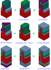
Figure 1 displays the major integration (process) steps for a proposed SABC scheme. The process steps are like those used during a typical GAA logic process manufacturing flow.
Study Methodology
The team ran multiple virtual fabrication experiments that varied the smallest critical dimensions (CD), overlay, and over-etch amount of the through-silicon via (TSV).
Virtual measurements were taken of the number of opens and shorts generated (number of nets in the structure), high-k damage (high-k material volume change), and the backside contact area of the typical structure.
The manufacturing success criteria were specified as follows:
- Backside contact area (CT to epitaxy): ≥150 nm2
- High K damage: <20 nm3
- No contact with the metal gate shorts
Using these criteria, the results of each virtual experiment in the DOE were classified as a “pass” or “failure” event.
SABC Indicates Higher Yield for Advanced Logic Nodes
The DOE results are shown in Figure 2 as a set of process window contour diagrams at various CD, overlay, and over-etch amounts for both the SABC and DBC contact schemes. The green areas in Figure 2 represent “pass” results, while the red areas represent “fail” events.
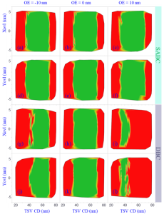
Due to its self-aligned capabilities, the SABC approach exhibits a much larger process window (larger green area) than the DBC architecture.
The DBC process window is very narrow, especially when the TSV is 10 nm over- or under-etched. The TSV failure exhibits itself as high-k damage, source-drain to metal gate shorts caused by excessive over-etching, small contact areas created by TSV under-etch and increased EPE caused by a larger TSV CD and additional overlay errors.
The virtual study demonstrated that the SABC approach to backside power minimizes EPE and over-etch variations in the TSV process and provides a much larger and more stable process window than a DBC approach. SABC is promising for use at advanced logic nodes and may support further logic device scaling.