HomePress ReleaseIndia Set to Welcome Three New Semiconductor Facilities and AMD's Design Center

    India Set to Welcome Three New Semiconductor Facilities and AMD’s Design Center

    In a recent announcement, the Union Minister for Electronics and IT, Ashwini Vaishnaw, disclosed that India is poised to witness the establishment of three state-of-the-art semiconductor fabrication facilities, attracting an estimated investment ranging between $8-12 billion. The minister highlighted ongoing discussions with the governments of Tamil Nadu, Telangana, Gujarat, and Karnataka for the establishment of these facilities, alongside AMD’s launch of an international design center in Bengaluru.

    Vaishnaw emphasized the potential of this burgeoning sector, characterizing it as a new industry for the country that will significantly contribute to the evolving manufacturing landscape of electronics, telecom, and defense electronics. Micron Technology’s investment announcement in June 2023, coupled with the initiation of facility construction in September, has instilled considerable confidence in India’s semiconductor mission.

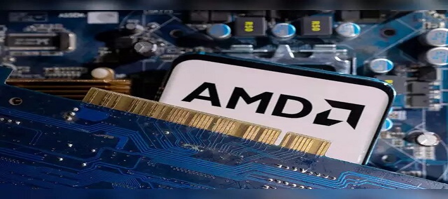
    The development also includes AMD’s strategic move to inaugurate a design center in Bengaluru, employing approximately 3,000 engineers. This center will exclusively focus on advancing semiconductor technology in areas such as machine learning, 3D stacking, and artificial intelligence. AMD’s substantial investment of $400 million over the next five years further solidifies its commitment to India.

    According to an AMD spokesperson, the new research and development (R&D) center will serve as a center of excellence, concentrating on the development of various products, including high-performance CPUs for data centers and PCs, gaming GPUs (graphics processing units), and adaptive SoCs (system-on-chip) and FPGAs (field-programmable gate arrays) for embedded devices. The design center, initiated in 2004, currently hosts only 25 percent of AMD’s international workforce.

    Saurabh Bhuria
    Saurabh Bhuriahttps://www.eletimes.ai/
    Saurabh Bhuria is a distinguished Technology Journalist associated with ELEtimes.com and TimesEV.com. With expertise in researching, writing, and editing, he demonstrates a deep understanding of technology, particularly in the EV industry. His continuous updates on EV, Automotive, and E-mobility industries reflect his commitment to staying at the forefront of emerging trends.

    Related News

    Must Read

    ROHM Strengthens Supply Capability for GaN Power Devices

    Combining TSMC’s Process Technology to Build an End-to-End, In-Group...

    element14 Community launches smart security and surveillance design challenge

    element14, an Avnet Community, in collaboration with ADI, has...

    R & S and LITEON demonstrate high‑throughput 5G femtocell testing with the PVT360A

    Rohde & Schwarz and LITEON collaborate to showcase a...

    Infineon presents MCU and sensor solutions for the future of AI, IoT, mobility, and robotics

    Next-generation embedded systems are essential for applications in the...

    R&S advances AI-RAN testing using digital twins in collaboration with NVIDIA

    Rohde & Schwarz will showcase a new milestone in...

    Top Seven Tech Trends in the semiconductor sector for 2026

    By: STMicroelectronics In 2026, a new class of intelligent machines...

    Keysight launches next-gen Infiniium XR8 Oscilloscopes for faster analysis, clearer insights, and a compact design

     Keysight Technologies introduced its next-generation Infiniium XR8 Real-Time oscilloscopes,...

    R&S showcases its comprehensive embedded systems test solutions at embedded world 2026

    Rohde & Schwarz will present its advanced test and...