Wearable technology has exploded in recent years. Spurred by advances in flexible sensors, transistors, energy storage, and harvesting devices, wearables encompass miniaturized electronic devices worn directly on the human skin for sensing a range of biophysical and biochemical signals or, as with smart watches, for providing convenient human-machine interfaces.
Engineering wearables for optimal skin conformity, breathability, and biocompatibility without compromising the tunability of their mechanical, electrical, and chemical properties is no small task. The emergence of electrospinning—the fabrication of nanofibers with tunable properties from a polymer base—is an exciting development in the field.


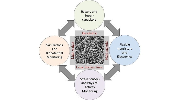
Researchers from Tufts University examined some of the latest advances in wearable electronic devices and systems being developed using electrospinning.
“We show how the scientific community has realized many remarkable things using electrospun nanomaterials,” said author Sameer Sonkusale. “They have applied them for physical activity monitoring, motion tracking, measuring biopotentials, chemical and biological sensing, and even batteries, transistors, and antennas, among others.”
Sonkusale and his colleagues showcase the many advantages electrospun materials have over conventional bulk materials.
Their high surface-to-volume ratio endows them with enhanced porosity and breathability, which is important for long-term wearability. Also, with the appropriate blend of polymers, they can achieve superior biocompatibility.
Conductive electrospun nanofibers provide high surface area electrodes, enabling both flexibility and performance improvements, including rapid charging and high energy storage capacities.
“Also, their nanoscale features mean they adhere well to the skin without the need for chemical adhesives, which is important if you are interested in measuring biopotentials, like heart activity using electrocardiography or brain activity using electroencephalography,” said Sonkusale.
Electrospinning is considerably less expensive and more user-friendly than photolithography for realizing nanoscale transistor morphologies with superior electronic transport.
The researchers are confident electrospinning will further establish its claim as a versatile, feasible, and inexpensive technique for the fabrication of wearable devices in the coming years. They note there are areas for improvement to be considered, including broadening the choice of materials and improving the ease of integration with human physiology.
They suggest the esthetics of wearables may be improved by making them smaller and, perhaps, with the incorporation of transparent materials, “almost invisible.”