

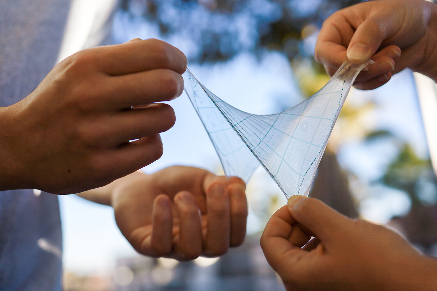
A team of researchers at Stanford have spent nearly two decades trying to develop skin-like integrated circuits that can be stretched, folded, bent and twisted—working all the while—and then snap back without fail, every time. Such circuits presage a day of wearable and implantable products, but one hurdle has always stood in the way.
The team think they have a solution. In a new study, the group describes how they have printed stretchable-yet-durable integrated circuits on rubbery, skin-like materials, using the same equipment designed to make solid silicon chips—an accomplishment that could ease the transition to commercialization by switching foundries that today make rigid circuits to producing stretchable ones.



The process allowed the researchers to squeeze more than 40,000 transistors in a single square centimetre of stretchable circuitry, but the team thinks double that number is within reach. While that would still be a far cry from the billions of transistors that can be squeezed into the same area on silicon chips, it would be enough to create simple circuits for on-skin sensors, body-scale networks and implantable bioelectronics with applications yet to be imagined.
“Our method improves elastic-transistor density by more than 100 times what anyone else has achieved so far. And it does it with excellent uniformity in the transistors while sacrificing nothing in electronic or mechanical performance,” said the researcher.
Old process, new chemistry
A major advantage of the Stanford process is that it can be done with the same equipment used to make silicon chips today. The process, known as photolithography, uses ultraviolet (UV) light to transfer an intricate, electrically active geometric pattern—a circuit—onto a solid substrate, layer by layer. It’s a complex, multistep process of coating, exposing with light, chemical etching and rinsing that leaves behind the all-important circuit.
This method has worked for decades in the semiconductor industry but, to date, the chemicals used to dissolve and wash away the light-resistant materials also wash away the skin-like polymers that are the foundation of stretchable circuits. By developing new photochemistries that work on these stretchable materials, Bao’s team is teaching tried-and-true manufacturing equipment to do new tricks. In fact, the Stanford process even does away with some of the steps necessary in silicon manufacturing. It all adds up to a remarkable result.
Dense and durable
The team used the new process to produce flexible circuits of roughly the same electrical performance as transistors used for current computer displays—useful for practical applications—then tested their materials for durability and performance. Stretching the circuits to double their original dimensions, both parallel and perpendicular to the circuit direction, the newly printed materials showed no cracks, delamination or, most importantly, the decline in function. Electrically, the transistors remained stable, even after 1,000 repeated stretches.

