
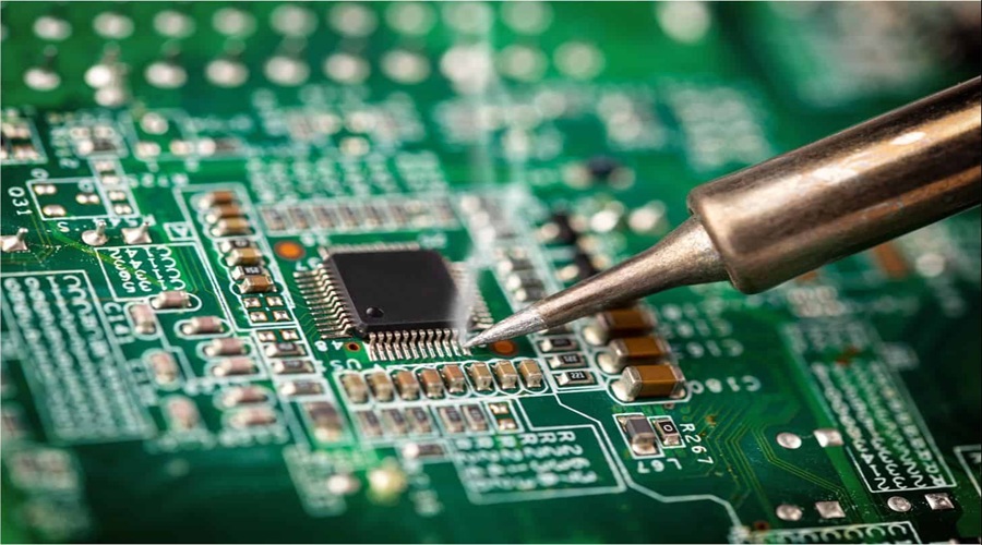
What is PCB Soldering?
Printed Circuit Board (PCB) soldering is a fundamental process in electronics manufacturing, where electronic components are securely attached to a PCB using molten solder. This process ensures electrical conductivity and mechanical stability, allowing components to function properly within a circuit. Soldering plays a crucial role in assembling various electronic devices, from consumer gadgets to industrial and automotive electronics.
How PCB Soldering Works
PCB soldering involves heating a metal alloy (solder) until it melts and flows into the joints between the electronic components and the copper traces of the PCB. As the solder cools, it solidifies, creating a strong electrical and mechanical connection. The process requires precision to avoid short circuits or weak connections that could lead to malfunctioning circuits.




There are two primary types of PCB soldering: Through-Hole Soldering (THS) and Surface Mount Soldering (SMS). Through-hole soldering involves inserting component leads into drilled holes on the PCB and then soldering them, whereas surface mount soldering involves mounting components directly onto the PCB surface without the need for drilled holes.
PCB Soldering Process
The soldering process involves multiple steps to ensure a reliable connection between the PCB and its components. Here’s a breakdown of the process:
- Preparation: The PCB surface and component leads are cleaned to remove any oxidation, dust, or residues that may interfere with soldering.
- Applying Flux: Flux is used to facilitate solder flow and prevent oxidation during the soldering process. It helps create a strong bond between the solder and the PCB.
- Heating: A soldering iron, reflow oven, or wave soldering machine heats the solder to its melting point. The temperature control is crucial to avoid damaging the PCB or components.
- Applying Solder: The molten solder is applied to the component joints, ensuring even distribution for a strong connection.
- Cooling and Solidification: Once the solder cools, it hardens, forming a durable electrical and mechanical bond between the PCB and the components.
- Inspection and Testing: The solder joints are inspected for defects such as cold joints, solder bridges, or incomplete connections. Automated testing may also be performed to verify electrical functionality.
Uses and Applications of PCB Soldering
PCB soldering is a vital process across various industries, enabling the production of a wide range of electronic devices. Some common applications include:
- Consumer Electronics: Smartphones, laptops, televisions, and gaming consoles rely on PCB soldering for compact and reliable electronic circuits.
- Automotive Electronics: Modern vehicles incorporate sophisticated electronic control units (ECUs), sensors, and infotainment systems, all assembled using PCB soldering.
- Industrial Automation: Robotics, control systems, and automation equipment depend on PCB soldering for precision and durability.
- Medical Devices: Advanced medical equipment, such as pacemakers, MRI machines, and diagnostic tools, require high-quality PCB soldering for safety and performance.
- Aerospace and Defense: High-reliability PCB soldering is essential in avionics, military-grade electronics, and space applications, where precision and durability are critical.
Advantages of PCB Soldering
PCB soldering offers several benefits that make it indispensable in electronics manufacturing:
- Strong Electrical Connections: Ensures reliable signal transmission and minimal electrical resistance.
- Compact and Lightweight Designs: Surface mount soldering allows for miniaturization of electronic devices without compromising performance.
- Mass Production Efficiency: Automated soldering techniques enable large-scale manufacturing with consistent quality and precision.
- Enhanced Durability: Well-soldered components withstand mechanical stress, temperature variations, and environmental factors.
- Cost-Effectiveness: Soldering allows for efficient assembly, reducing production costs in electronics manufacturing.
Disadvantages and Challenges of PCB Soldering
Despite its advantages, PCB soldering comes with some challenges and limitations:
- Thermal Stress on Components: Excessive heat during soldering can damage sensitive components, affecting their lifespan.
- Solder Defects: Issues such as cold joints, solder bridges, or voids can lead to circuit failures and require rework.
- Environmental Concerns: Traditional lead-based solder poses environmental and health risks, necessitating the use of lead-free alternatives.
- Complexity in Multi-Layer PCBs: Soldering advanced PCBs with multiple layers and fine-pitch components requires high precision and expertise.
- Initial Setup Cost: Advanced soldering equipment, such as reflow ovens and wave soldering machines, can be expensive for small-scale manufacturers.
Conclusion
PCB soldering is a critical process that enables the manufacturing of modern electronic devices. With advancements in soldering techniques and materials, manufacturers can achieve high-quality, reliable electronic assemblies. As the industry moves towards lead-free and automated soldering solutions, innovation in PCB soldering will continue to drive the evolution of electronic technology.

