When most people think of wearable devices, they think of smart watches, smart glasses, fitness trackers, even smart clothing. These devices, part of a fast-growing market, have two things in common: They all need an external power source, and they all require exacting manufacturing processes. Until now.
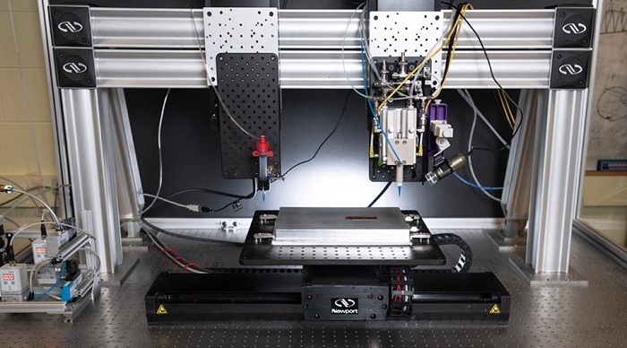
Yanliang Zhang, associate professor of aerospace and mechanical engineering at the University of Notre Dame, and doctoral student Yipu Du have created an innovative hybrid printing method—combining multi-material aerosol jet printing and extrusion printing—that integrates both functional and structural materials into a single streamlined printing platform.


Zhang and Du, in collaboration with a team at Purdue University led by professor Wenzhuo Wu, also have developed an all-printed piezoelectric (self-powered) wearable device.
Using their new hybrid printing process, the team demonstrated stretchable piezoelectric sensors, conformable to human skin, with integrated tellurium nanowire piezoelectric materials, silver nanowire electrodes and silicone films. The devices printed by the team were then attached to a human wrist, accurately detecting hand gestures, and to an individual’s neck, detecting the individual’s heartbeat. Neither device used an external power source.
Piezoelectric materials are some of the most promising materials in the manufacture of wearable electronics and sensors because they generate their own electrical charge from applied mechanical stress instead of from a power source.
Yet printing piezoelectric devices is challenging because it often requires high electric fields for poling and high sintering temperatures. This adds to the time and cost of the printing process and can be detrimental to surrounding materials during sensor integration.
“The biggest advantage of our new hybrid printing method is the ability to integrate a wide range of functional and structural materials in one platform,” said Zhang.
“This streamlines the processes, reducing the time and energy needed to fabricate a device, while ensuring the performance of printed devices.”
Vital to the design, said Zhang, are nanostructured materials with piezoelectric properties, which eliminate the need for poling or sintering, and the highly stretchable silver nanowire electrodes, which are important for wearable devices attached to bodies in motion.
“We’re excited to see the wide range of opportunities that will open up for printed electronics and wearable devices because of this very versatile printing process,” said Zhang.