
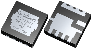
The design of future power electronic systems is continuously pushed to improve state-of-the-art performance and power density. Supporting this trend, Infineon Technologies AG launches a new Source-Down 3.3 x 3.3 mm² PQFN product family in the 25-150 V classes with Bottom-Side (BSC) and Dual-Side Cooling (DSC) variants. The new product family provides significant enhancements on the component level to offer attractive solutions in DC-DC power conversion, opening up new possibilities for system innovation in server, telecom, OR-ing, battery protection, power tools, and charger applications.
The new portfolio combines Infineon’s latest MOSFET technology with leading-edge packaging to bring system performance to the next level. In the Source-Down (SD) concept, the MOSFET die source contact is flipped toward the footprint side of the package, which is then soldered to the PCB. In addition, the concept comprises an improved clip design on top of the chip for the drain contact and market-leading chip-to-package area ratio.




As system form factors continuously shrink, two key aspects are essential: reduction of power losses and optimal thermal management. Compared to best-in-class PQFN 3.3 x 3.3 m² Drain-Down devices, the new family significantly improves the on-resistance (RDS(on)) by up to 25 percent. Infineon’s OptiMOS Source-Down PQFN with Dual-Side Cooling provides an enhanced thermal interface to redirect power losses from the switch towards the heatsink. Dual-Side Cooling variants offer the most direct way to connect a power switch to a heatsink, increasing power dissipation capability by a factor of up to three compared to the corresponding Bottom-Side Cooled Source-Down variant.
Two different footprint variants are available to offer the highest flexibility for PCB routing. A traditional Standard-Gate variant provides a quick and easy modification of existing Drain-Down designs. And a Center-Gate (CG) variant opens new possibilities for paralleling devices to keep the driver-to-gate connection as short as possible. With an outstanding continuous current capability of up to 298 A, the entire OptiMOS Source-Down PQFN 3.3 x 3.3 mm² 25-150 V product family enables the highest system performance.

