
Courtesy: Teradyne
Artificial intelligence (AI) is transforming industries, enhancing our daily lives, and improving efficiency and decision-making, but its need for computing power is growing at an astonishing rate, doubling every three months (Figure 1). To maintain this pace, the semiconductor industry is moving beyond traditional chip development – it has entered the era of heterogeneous chiplets in advanced integrated packages.


The Rise of Chiplets
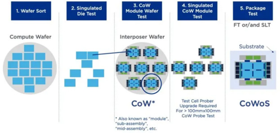
Chip companies like NVIDIA and AMD are rewriting the rules, designing architectures that combine multiple CPUs and GPUs in a single advanced package along with high bandwidth memory (HBM). AI workloads require rapid access to vast amounts of data, made possible by integrating HBMs. This approach, combining two, four, or more processing cores with HBM stacks, requires a complex, advanced packaging technique developed by TSMC called CoWos® – Chip-on-Wafer-on-Substrate, typically referred to as 2.5/3D packaging (Figure 2). These packages can exceed 100 mm x 100 mm in size and will require wafer interposer probers that can handle large CoW modules/stacks and also meet significantly larger thermal dissipation requirements, as discussed below.
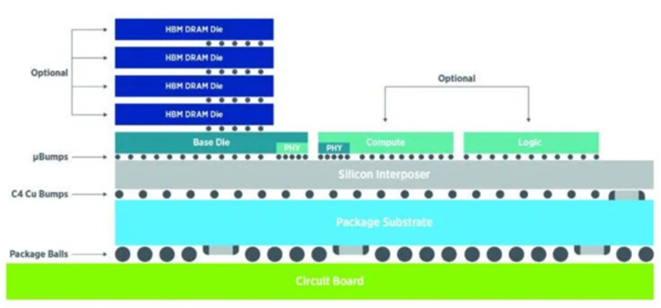
To maintain peak performance, these heterogeneously integrated advanced packaging devices need proprietary high-speed interfaces to communicate efficiently. All these requirements contribute to an increasingly complex semiconductor landscape.
Testing Becomes More Complex in Step with Chip Advancements
As package complexity increases, so does the need for more deliberate test strategies. In the transition from monolithic dies to chiplets, long-established test methods are not always directly transferable because test IP is now distributed across multiple dies and, in some cases, across different design teams or companies. This fragmentation requires a clearer definition of what must be tested at each stage—die, bridge, interposer, substrate, and stack—and which standards or techniques apply to each scope.
Packing multiple dies into a single chiplet-based system is a major advancement, but it raises a key challenge: verifying that every component functions correctly before final assembly. Multi-die packages require rigorous screening to avoid yield loss, and it is not enough to qualify only the dies. Interposers, substrates, bridges, and stacks also need to be validated, using test techniques appropriate to each layer. The industry is thus moving into “known-good-everything”, from known-good-die (KGD) to known-good-interposer (KGI), to known-good-CoW (KG-CoW), and so on. (Figure 3)
High-speed communication between chiplets introduces an additional layer of complexity. Dies must exchange data at extreme speeds – such as during GPU-to-HBM transfers – yet their physical and electrical interfaces vary by manufacturer. Open standards like Universal Chiplet Interconnect Express (UCIe™) continue to evolve, but chiplet interfaces still differ widely. To support this diversity, test solutions increasingly need interface IP that behaves like the device’s native protocol to avoid electrical overstress or probe-related damage. Some suppliers now offer UCIe-compliant PHY and controller IP that device makers can integrate, enabling automated test equipment (ATE) platforms to test high-speed links safely and consistently.
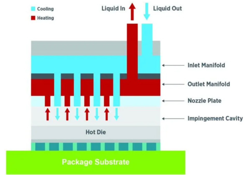
Manufacturers and test operators must also pay close attention to thermal management. More processing power means more heat dissipation issues, requiring advanced cooling methods – perhaps even liquid cooling inside the package itself (Figure 4). More die in the package means more connections, and thus, more resources are needed in the tester. More transistors mean higher power supply current requirements, more power supply instruments, and an increased set of thermal challenges that demand innovative cooling solutions and advanced adaptive thermal control (ATC) strategies.
Lastly, manufacturing test operations must consider the interposer, a physical interface layer that electrically connects a chip to a substrate or other active component. For example, a multilayer or 2.5D package includes multiple dies on an interposer assembled on top of a substrate. That interposer functions as a mini silicon board, routing signals from the upper floor die to the bottom floor die. It’s critical that the interposer is also a known good die or known good interposer (KGI) to ensure adequate yields for advanced packages.
The Future of AI and Semiconductor Testing
There has been an uptick in industry recognition that semiconductor testing is an integral part of today’s chiplet and advanced packaging trend. As this unfolds, AI computing will continue its pace of unprecedented evolution, relying on semiconductor testing to fill a crucial role in ensuring quality devices get to market in the shortened timelines today’s market demands. Semiconductor test will remain the unsung hero of AI-driven computing, steadily enabling the next wave of technological breakthroughs.