
By Tzu-Yi Lee
Revolutionizing semiconductor fabrication, ALD, ALE, and NBE deliver atomic-scale precision, driving unprecedented performance and scalability in next-generation miniaturized devices.


Introduction
With the rapid growth of the semiconductor industry, Moore’s law has become a core guiding principle for the continuous advancement of electronic devices. Moore’s law predicts that the number of transistors will double every two years, a trend that is driving the continued reduction in device and circuit size. As the size of semiconductor devices shrinks further, the complexity and accuracy of the manufacturing process increase dramatically, requiring the introduction of ultra-precision and ultra-fine technologies into the semiconductor process to ensure device performance and reliability. Among these technologies, etching and deposition are particularly crucial as they form the foundation for achieving high-performance semiconductor devices. They play an essential role in enabling device miniaturization and increasing functional density. Fig. illustrates the trend in semiconductor manufacturing technology from 2000 to 2035, reflecting advancements beyond Moore’s law and incorporating more-than-Moore principles. As transistor technology evolves to Integrated Circuit (IC) evolves, we can see a progression from scale devices and wires to scale basic logic units to scale system functions. Early developments in transistor technology, such as geometric scaling at the 90 nm node, included introducing strained Si and using copper (Cu) for back-end-of-line (BEOL) interconnections. Over time, technological advances drove transistors to 40 nm and 28 nm nodes, when the use of high-k gate dielectrics and metal gate technologies appeared, marking the era of equivalent scaling. With the further development of process technology, from 20 nm to 7 nm, transistor technology entered the era of heterogeneous scaling (post-Moore scaling), which included the widespread use of fin field-effect transistors (FinFETs). FinFETs provide superior channel control due to their three-dimensional structure, which allows the gate to surround the channel on multiple sides, enhancing gate control and reducing short-channel effects. In recent years, the introduction of gate-all-around (GAA) transistors, an advanced technology, has further shrunk device size and provided better control of short-channel effects, reduced leakage current, and enhanced switching performance. As technology nodes advance to 5 nm and beyond, innovations such as GAA transistors provide better control of short-channel effects, reduced leakage, and enhanced performance. Future scaling is expected to incorporate compound field-effect transistors (CFETs), 2D semiconductors, and hybrid integration, which not only sustain Moore’s law but also expand into more-than-Moore functionalities, such as photonic integration, quantum technologies, and neuromorphic computing. These advancements heavily rely on nanoscale etching and deposition processes, such as atomic layer deposition (ALD), atomic layer etching (ALE), and neutral beam etching (NBE), which are critical in achieving the precision and performance required for next-generation devices. This article shows how these advanced techniques drive semiconductor fabrication, supporting continued progress and enabling breakthroughs beyond Moore’s law.
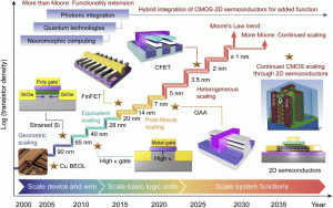
Fig. 1. Evolution of transistor density and gate length in ICs.
Definition and background
The etching process involves removing a material from a surface through chemical or physical methods, which typically plays a key role in semiconductor manufacturing. Precise control of this process, including major factors such as etch depth, etch profile, surface roughness, and uniformity, is critical to ensuring the performance and reliability of micro- and nanoelectronic devices. Wet etching, which utilizes a chemical reaction in a bath environment, is known for its low cost, ease of implementation, and high material selectivity. Conversely, dry etching is performed through physical and chemical reactions in a vacuum chamber, providing greater precision depth control, profile selectivity, and the ability to define critical feature dimensions.
Atomic layer etching (ALE)
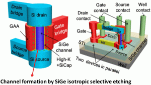
ALE is a highly precise technique critical for fabricating nanoscale semiconductor devices. By alternating between adsorption and reaction steps, ALE achieves the removal of single atomic layers per cycle, providing exceptional control and minimizing surface roughness. This method, derived from ALD techniques, involves sequential exposure to different reactive gases, with intermediate purging steps to ensure precise layer-by-layer removal and maintain atomic-scale accuracy. ALE is particularly advantageous in the fabrication of advanced 3D integrated circuits (3D ICs) and memory devices. In 3D IC manufacturing, ALE addresses the challenges of creating complex 3D transistor architectures, such as GAA and multi-bridge-channel FETs (MBCFETs). By enabling atomic-scale etching, ALE provides exceptional control over morphology and depth, ensuring precise patterning for nanoscale features.
Neutral-beam etching (NBE)
NBE represents a significant advancement in the etching processes for GaN-based HEMTs and light-emitting diodes (LEDs). This method effectively addresses the critical challenge of plasma-induced damage, which is prevalent in conventional etching techniques such as ICP-RIE. GaN materials are highly valued in the semiconductor industry for high-power and high-frequency applications. However, achieving normally-off operation in GaN-based HEMTs remains challenging due to the plasma-induced damage associated with techniques such as gate recessing. NBE offers a potential solution to minimize such damage and enhance device performance.
Deposition techniques
Thin film technology is an advanced approach aimed at improving the structural, electrical, magnetic, optical, and mechanical properties of bulk materials. It has found widespread application in semiconductor devices, integrated circuits, transistors, liquid crystal displays, light-emitting diodes, solar cells, sensors, and micro-electromechanical systems (MEMSs). The distinctive properties of thin film materials are crucial for the technological advancement of various electronic, electrical, magnetic, and optical devices. These films are created using various physical or chemical methods, each of which is essential for producing ultra-thin materials known for their uniform, conformal, and controllable thickness. As atomic and near-atomic scale manufacturing (ACSM) evolves, the necessity of depositing high-quality, impurity-free thin films for laminated structures becomes crucial.
The future of ALD, ALE, and NBE technologies is promising as ongoing advancements continue to address the evolving demands of semiconductor manufacturing. Numerous optimization strategies have been employed to enhance their precision and efficiency. In particular, controlling deposition thickness in ALD, achieving atomic-level etching with ALE, and minimizing surface damage through NBE have proven crucial for improving device performance. Geometrical parameters such as layer thickness, etch depth, and surface passivation have significant impacts on device reliability and durability. Addressing thermal management, particularly in high-power applications, becomes essential as devices scale further. Future efforts could explore the use of more thermally conductive substrates and the refinement of etching profiles to minimize defects and improve device performance. Additionally, optimizing contact technologies to reduce resistance and ensure smooth surface morphology will be critical. Looking ahead, further research should focus on enhancing the uniformity and precision of these processes for advanced applications in micro-LEDs, high-speed communications, and optoelectronics. Future research should consider the performance capabilities of ALD, ALE, and NBE technologies to promote the development of next-generation semiconductor devices.