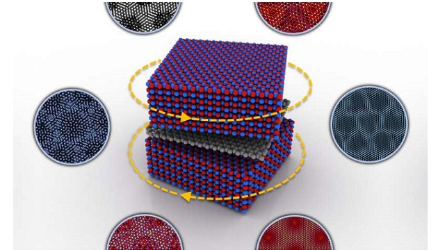
A recent study from the labs of James Hone (mechanical engineering) and Cory Dean (physics) demonstrates a new way to tune the properties of two-dimensional (2D) materials simply by adjusting the twist angle between them. The researchers built devices consisting of monolayer graphene encapsulated between two crystals of boron nitride and, by adjusting the relative twist angle between the layers, they were able to create multiple moiré patterns.
Moiré patterns are of high interest to condensed matter physicists and materials scientists who use them to change or generate new electronic material properties. These patterns can be formed by aligning boron nitride (BN, an insulator) and graphene (a semimetal) crystals. When these honeycomb lattices of atoms are close to alignment, they create a moiré superlattice, a nanoscale interference pattern that also looks like a honeycomb. This moiré superlattice alters the quantum mechanical environment of the conducting electrons in the graphene, and therefore can be used to program significant changes in the observed electronic properties of the graphene.
To date, most studies on the effects of moiré superlattices in graphene-BN systems have looked at a single interface (with either the top or bottom surface of the graphene considered, but not both). However, a study published by Hone and Dean last year demonstrated that total rotational control over one of the two interfaces was possible within a single device.
By designing a device that has persistent alignment at one interface, and tunable alignment at the other, the Columbia team has now been able to study the effects of multiple moiré superlattice potentials on a layer of graphene.
“We decided to look at both the top and bottom surfaces of the graphene in a single nanomechanical device,” said Nathan Finney, a PhD student in Hone’s lab and co-lead-author of the paper, published online September 30 by Nature Nanotechnology and now the cover story of the November print edition. “We had a hunch that by doing so, we would be able to potentially double the strength of the moiré superlattice using the coexisting moiré superlattices from the top and bottom interfaces.”
The team discovered that twisting the angle of the layers enabled them to control both the strength of the moiré superlattice as well as its overall symmetry, inferred from the significant changes in the electronic properties of the graphene observed.
At angles close to alignment, a highly altered graphene band structure emerged, observable in the formation of coexisting non-overlapping long-wavelength moiré patterns. At perfect alignment, the graphene’s electronic gaps were either strongly enhanced or suppressed, depending on whether the top rotatable BN was twisted 0 or 60 degrees. These changes in the electronic gaps corresponded to the expected changes in symmetry for the two alignment configurations, inversion symmetry broken at 0 degrees, and inversion symmetry restored at 60 degrees.
“This is the first time anyone has seen the full rotational dependence of coexisting moiré superlattices in one device,” Finney notes. “This degree of control over the symmetry and the strength of moiré superlattices can be universally applied to the full inventory of 2D materials we have available. This technology enables the development of nanoelectromechanical sensors with applications in astronomy, medicine, search and rescue, and more.”
The researchers are now refining the ability to twist monolayers of a wide range of 2D materials to study such exotic effects as superconductivity, topologically induced ferromagnetism, and non-linear optical response in systems that lack inversion symmetry.


