HomeTechnologyPhotonics3D Design Leads to First Stable and Strong Self-Assembling 1D Nanographene Wires

    3D Design Leads to First Stable and Strong Self-Assembling 1D Nanographene Wires

    Nanographene is flexible, yet stronger than steel. With unique physical and electronic properties, the material consists of carbon molecules with only one atom thick arranged in a honeycomb shape. Still early in technological development, current fabrication methods require the addition of substituents to obtain a uniform material. Additive-free methods result in flimsy, breakable fibers—until now.

    An international team of researchers has developed self-assembling, stable, and strong nanographene wires. The team set out to synthesize curved, infinitely stacking nanographene—like potato chips in a cardboard can—that can assemble into nanowires.

    Effectively stacked hydrocarbon wires have the potential to be used as a variety of nano-semiconductor materials. Previously, it has been necessary to introduce substituents that are not related to or inhibit the desired electronic function in order to control the assembly of the wires.

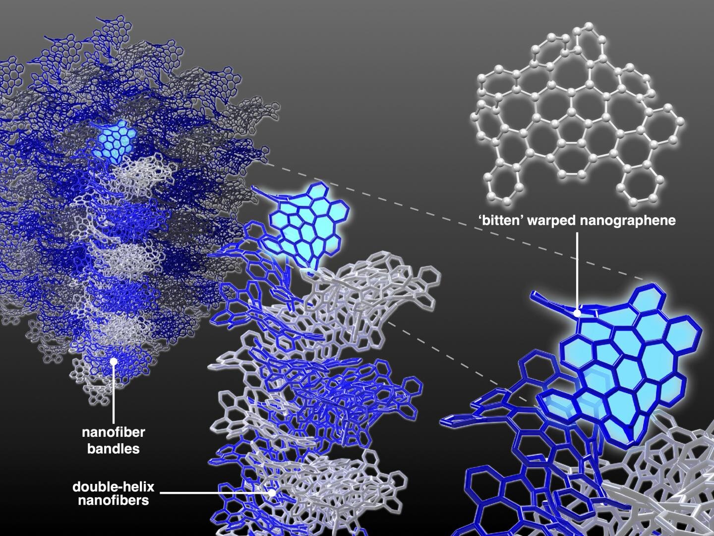
    By removing substituents, or additives, from the fabrication process, researchers can develop molecular materials that have a specific, desired electronic function. With this goal in mind, the team developed a molecule called ‘bitten’ warped nanographene (bWNG), with 68 carbon atoms and 28 hydrogen atoms forming a ‘bitten apple’ shape. Created as a solution, when left to evaporate over 24 hours in the presence of hexane—an ingredient in gasoline with six carbon atoms—bWNG becomes a gel.

    The researchers attempted to recrystallize the molecules of the original solution to examine the specific structure of the bWNG gel through X-ray crystallography. This technique can reveal the atomic and molecular structure of a crystal by irradiating the structure with X-rays and observing how they diffract.

    They attempted recrystallizing many times to determine the structure, but it grew to only a few hundred nanometers, noting that this size is much too small for X-ray crystallography. It was only by electron diffraction, a new method for determining the structure of organic materials, that they were able to analyze the structure.

    Electron diffraction is similar to X-ray crystallography, but it uses electrons instead of X-rays, resulting in a pattern of interference with the sample material that indicates the internal structure.

    They found that the bWNG gel consisted of double-stranded, double-helix nanofibers that assembled themselves from curved, stackable nanographene.

    The structure of the nanofibers is a double-stranded double helix, which is very stable and, therefore, strong. Next, we would like to realize a semiconductor wire made entirely of carbon atoms.
    ELE Times Research Desk
    ELE Times Research Deskhttps://www.eletimes.ai
    ELE Times provides extensive global coverage of Electronics, Technology and the Market. In addition to providing in-depth articles, ELE Times attracts the industry’s largest, qualified and highly engaged audiences, who appreciate our timely, relevant content and popular formats. ELE Times helps you build experience, drive traffic, communicate your contributions to the right audience, generate leads and market your products favourably.

    Related News

    Must Read

    TI’s new power-management solutions enable scalable AI infrastructures

    Texas Instruments (TI) debuted new design resources and power-management...

    ESA awards Rohde & Schwarz for contributions to 30 years European Satellite Navigation

    The event brought together institutional and industrial partners, ESA...

    STMicroelectronics joins FiRa board, strengthening commitment to UWB ecosystem and automotive Digital Key adoption

    STMicroelectronics, a global semiconductor leader serving customers across the...

    STARLight Project chosen as the European consortium to lead in next-gen silicon photonics on 300 mm wafers

    The STARLight project is bringing together a consortium of leading...

    KYOCERA AVX RELEASES NEW KGP SERIES STACKED CAPACITORS

    KYOCERA AVX released the new KGP Series commercial-grade stacked...

    Microchip Unveils First 3 nm PCIe Gen 6 Switch to Power Modern AI Infrastructure

    Switchtec Gen 6 PCIe Fanout Switches deliver extra bandwidth,...

    Nuvoton Launches Arbel NPCM8mnx System-in-Package (SiP) for AI Servers and Datacenter Infrastructure

    Breakthrough BMC Innovation Powers Secure, Scalable, and Open Compute...

    NEPCON ASIA 2025: Showcasing the Future of Smart Electronics Manufacturing

    NEPCON ASIA 2025, taking place from October 28 to...

    Renesas Expands Sensing Portfolio with 3 Magnet-Free IPS ICs & Web-Based Design Tool

    New Simulation & Optimization Platform Enables Custom Coil Designs...

    IEEE IEDM, 2025 Showcases Latest Technologies in Microelectronics, Themed “100 Years of FETs”

    The IEEE International Electron Devices Meeting (IEDM) is considered...