Researchers from North Carolina State University used computational analysis to predict how optical properties of semiconductor material zinc selenide (ZnSe) change when doped with halogen elements, and found the predictions were confirmed by experimental results. Their method could speed the process of identifying and creating materials useful in quantum applications.
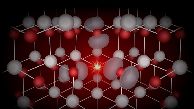
Creating semiconductors with desirable properties means taking advantage of point defects—sites within a material where an atom may be missing, or where there are impurities. By manipulating these sites in the material, often by adding different elements (a process referred to as “doping”), designers can elicit different properties.


“Defects are unavoidable, even in ‘pure’ materials,” says Doug Irving, University Faculty Scholar and professor of materials science and engineering at NC State. “We want to interface with those spaces via doping to change certain properties of a material. But figuring out which elements to use in doping is time and labour-intensive. If we could use a computer model to predict these outcomes it would allow material engineers to focus on elements with the best potential.”
In a proof of principle study, Irving and his team used computational analysis to predict the outcome of using halogen elements chlorine and fluorine as ZnSe dopants. They chose these elements because halogen-doped ZnSe has been extensively studied but the underlying defect chemistries are not well established.
The model analyzed all possible combinations of chlorine and fluorine at defect sites and correctly predicted outcomes such as electronic and optical properties, ionization energy and light emission from the doped ZnSe.
“By looking at the electronic and optical properties of defects in a known material, we were able to establish that this approach can be used in a predictive way,” Irving says. “So we can use it to search for defects and interactions that might be interesting.”
In the case of an optical material like ZnSe, changing the way the material absorbs or emits light could allow researchers to use it in quantum applications that could operate at higher temperatures since certain defects wouldn’t be as sensitive to elevated temperatures.
“Beyond revisiting a semiconductor like ZnSe for potential use in quantum applications, the broader implications of this work are the most exciting parts,” Irving says. “This is a foundational piece that moves us toward larger goals: using predictive technology to efficiently identify defects and the fundamental understanding of these materials that results from using this technology.”