Courtesy: Cadence
As three-dimensional integrated circuit (3D-IC) technology becomes the architectural backbone of AI, high-performance computing (HPC), and advanced edge systems, thermal management has shifted from a downstream constraint to a fundamental design driver. The dense vertical integration that enables unprecedented performance also concentrates heat at levels that traditional two-dimensional design methodologies cannot anticipate or mitigate. In fact, the temperatures and heat fluxes inside localised 3D-IC hotspots can approach fractions of those encountered in rocket-launching thermal zones, only here the challenge unfolds on a microscopic silicon landscape rather than within a combustion chamber. This extreme thermal intensity makes early and predictive planning essential rather than optional.


Effective thermal management now begins at the architecture definition stage, where designers evaluate stack feasibility, power distribution, and allowable thermal envelopes before committing to partitioning decisions. These early insights directly shape block placement, power-delivery topology, and the choice of materials, interposers, and packaging technologies. As the industry increasingly relies on vertically integrated systems to achieve performance-per-watt gains, thermal awareness emerges as an architectural discipline in its own right, one that guides every subsequent stage of the 3D-IC design flow.
This article guides modelling, estimating, and mitigating thermal challenges in dense stacks and interposer-based 3D-ICs, with an emphasis on early electrothermal strategies that scale with complexity.
Sources of Heat in Stacked Architectures
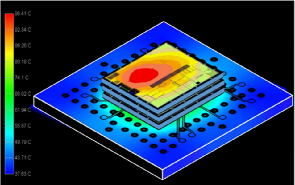
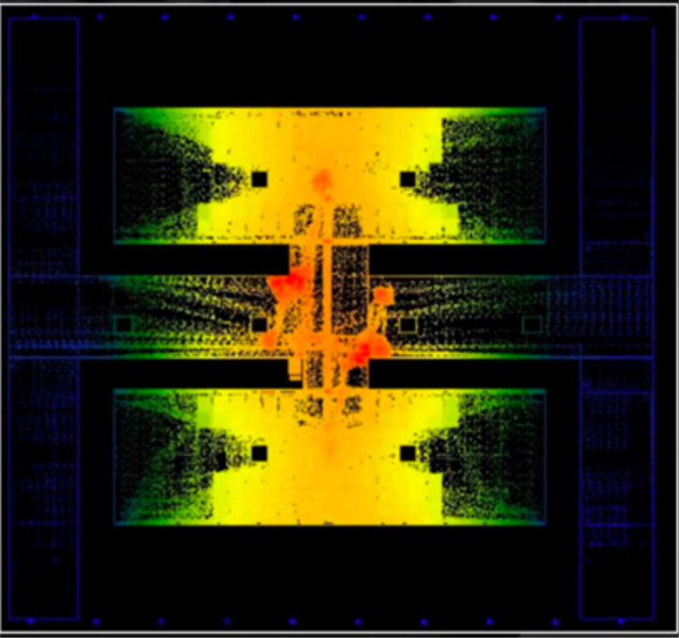
Heat in 3D-ICs arises from a combination of device activity, vertical power density, and material constraints. When logic, memory, and accelerators are stacked, the total power per unit footprint increases dramatically. Upper dies, which are furthest from the heatsink, experience higher thermal resistance and reduced cooling efficiency, creating natural hotspots even when their individual power numbers appear modest.
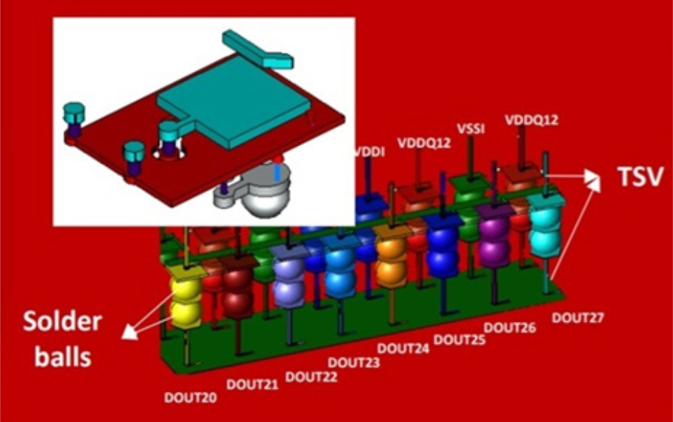
The placement of through-silicon via (TSV) arrays, micro-bumps, and interconnect pillars also shapes the heat landscape. These structures act not only as electrical conduits but also as thermal conduits, depending on the material and density. Die-to-die interfaces with bonding layers often introduce thermal bottlenecks, and when chiplets operate at different power states, steep thermal gradients can trigger stress and reliability concerns. Understanding these interactions early is essential for setting realistic thermal limits and performance expectations.
Early Compact Models and Power Map Estimation
Thermal analysis must begin in parallel with the architectural definition itself. Early-stage compact models enable architects to approximate temperature distributions using only high-level power budgets, long before physical implementation. By capturing the combined influence of die thickness, material stacks, bonding interfaces, and interposer conductivity, these models reveal whether planned power densities or proposed die-stack configurations are thermally realistic. They help flag infeasible assumptions early, ensuring that functional partitioning and stacking choices are guided by thermally credible boundaries rather than late-stage surprises.
Creating usable power maps at this stage does not require full register transfer level (RTL) activity vectors. Coarse workload profiles can yield first-order estimates of dynamic and leakage power. When combined with simplified geometry models, they highlight thermally sensitive regions, enabling design teams to adjust block partitioning, die assignment, and approximate placement before entering the detailed implementation phase.
Cadence’s multiphysics system analysis ecosystem connects power estimation, compact thermal model (CTM) modelling, and system-level thermal analysis, ensuring that signal, power, electromagnetic (EM), and thermal assumptions remain aligned throughout the early design phase. This early visibility reduces late-stage thermal surprises, which are often the costliest to rectify.
Heat Paths Through Dies, Interposers, and Package
Heat does not follow a single escape route in a 3D-IC. Instead, it propagates through a network of vertical and lateral paths whose efficiency depends on materials, die arrangement, and the package environment. Lower dies may benefit from direct contact with the heatsink, while upper dies rely on indirect conduction through intermediate layers. Thermal resistance builds cumulatively across each interface.
Interposers, whether made of silicon, glass, or organic materials, play a significant role in the heat flow picture. Silicon interposers offer superior thermal conductivity, enabling heat spreading but also concentrating thermal load where chiplets cluster. Organic interposers introduce more thermal resistance but offer other integration advantages. Achieving the correct tradeoff means modelling these layers as active participants in heat distribution, not static mechanical components.
The entire package, including substrate layers, heat spreaders, and lid materials, must also be included in thermal simulation. When package effects are omitted in early analysis, temperature predictions often skew optimistic, masking hotspots that emerge only after assembly-level modelling is performed.
Materials, TIMs, and Cooling Options for Stacks
Thermal simulation heavily relies on the structural definition of a product because the geometry, material properties, and assembly details directly dictate how heat is generated, transferred, and dissipated.
High-conductivity silicon, optimised interconnect materials, and improved underfill or bonding layers can lower the vertical thermal resistance of a stack. Thermal interface materials (TIMs) exhibit significant variations in performance, and even slight differences in thickness or coverage can result in substantial temperature differences across dies.
Cooling strategies for 3D-ICs are evolving rapidly. Traditional air cooling can be sufficient for moderate power budgets, but high-performance AI and HPC systems often require advanced approaches such as direct liquid cooling or vapour chamber solutions. The choice of cooling strategy should align with the power roadmap, not just the current generation’s requirements. Once a die stack is assembled, cooling options become constrained, so decisions made early influence the thermal feasibility of future product iterations.
Co-Optimisation with Placement and PDN Design
Thermal constraints directly influence floorplanning, macro placement, and power delivery network (PDN) topology in 3D-ICs. Efficient heat spreading is achieved when high-power blocks are positioned to maximise vertical conduction paths and lateral spreading through metal layers. If a block is placed too far from major thermal conduits, even robust cooling cannot compensate for the heat.
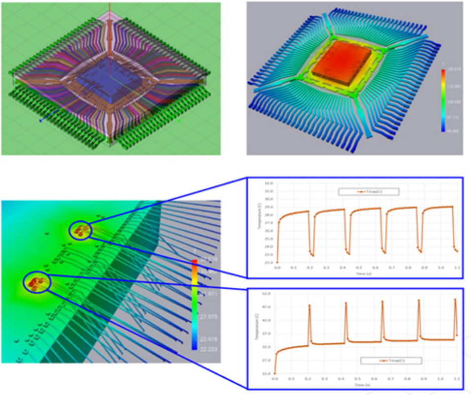
The PDN adds additional complexity. Power delivery structures, including TSVs, bumps, and interposer redistribution layers, introduce their own resistive heating. When modelled jointly with thermal effects, the combined electro-thermal behaviour reveals interactions that neither analysis can capture alone. Co-optimisation across these domains ensures that thermal mitigation does not compromise power integrity and vice versa.
A tightly integrated workflow enables round-trip refinement as power, placement, and package assumptions evolve. Without this iterative co-design, late-stage violations become inevitable, requiring disruptive redesigns.
Electro-Thermal Readiness for Signoff
Before committing a 3D-IC to final signoff, teams must verify that the design can withstand realistic thermal stress across operating modes and process corners. This includes validating that estimated power profiles align with actual activity, ensuring that predicted peak temperatures remain within safe limits, and confirming that no layer or interface exceeds its thermal reliability threshold.
Die-to-die boundaries, micro-bump arrays, TSV clusters, and package interconnects must be evaluated holistically, since minor thermal mismatches can accumulate into significant mechanical strain. Long-term reliability also depends on understanding how temperature interacts with electromigration, ageing, and performance drift over the product lifetime.
A complete electro-thermal signoff process provides the confidence needed before entering manufacturing, reducing field failures and ensuring long-term stability.
Designing for Thermal Scalability
3D-ICs deliver unprecedented performance, but they require a disciplined and predictive approach to thermal management. Success depends on treating heat as a first-order design variable, not a late-stage correction. Early modelling, accurate power estimation, careful material and stack selection, and co-optimisation across placement, PDN, interposer, and package all contribute to thermal resilience.
As system complexity continues to climb, teams that embed electro-thermal planning into their architecture and implementation flows will deliver higher-performing, more reliable, and scalable 3D-IC designs. Thermal awareness is no longer a specialisation; it is a foundational competency for next-generation semiconductor design.