Space-Saving Device Offers Low Max. RthJC of 0.36 °C/W and Wettable Flanks to Improve Thermal Performance and Solderability in Industrial Applications
To provide higher efficiency for industrial applications, Vishay Intertechnology, Inc. introduced a new 80 V TrenchFET Gen IV n-channel power MOSFET in the PowerPAK 8x8SW bond wireless (BWL) package with best-in-class on-resistance. Compared to competing devices in the same footprint, the Vishay Siliconix SiEH4800EW offers 15 % lower on-resistance while reducing RthJC by 18 %.
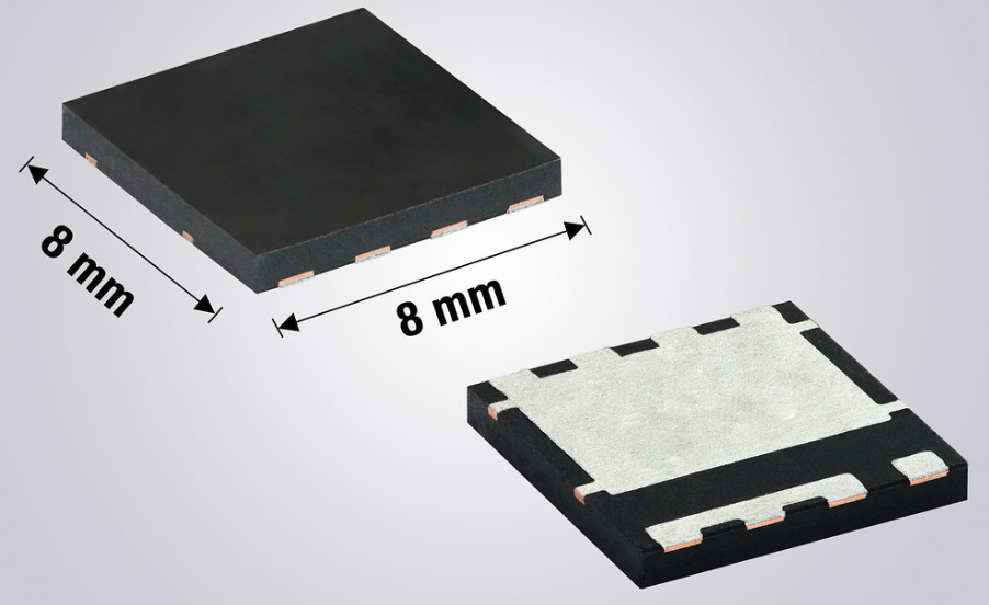
With on-resistance down to 0.88 mΩ typical at 10 V, the device released today minimizes power losses from conduction to increase efficiency while improving thermal performance with a low maximum RthJC of 0.36 °C/W. With its 8 mm by 8 mm footprint, the space-saving device occupies 50 % less PCB space than MOSFETs in the TO-263 package while offering an ultra-low profile of 1 mm.
The SiEH4800EW implements a fused lead to increase the source PAD solderable area to 3.35 mm², which is four times larger than a traditional PIN solder area. This decreases the current density between the MOSFET and PCB, reducing the risk of electro-migration risk and enabling a more robust design. In addition, the device’s wettable flanks enhance solderability while making it easier to visually inspect the reliability of solder joints.
The MOSFET is ideal for synchronous rectification and OR-ing functionality. Typical applications will include motor drive controls, power tools, welding equipment, plasma cutting machines, battery management systems, robotics, and 3D printers. In these applications, the device offers high-temperature operation to +175 °C, and its BWL design minimizes parasitic inductance while maximizing current capability.
RoHS-compliant and halogen-free, the MOSFET is 100 % Rg and UIS tested.


