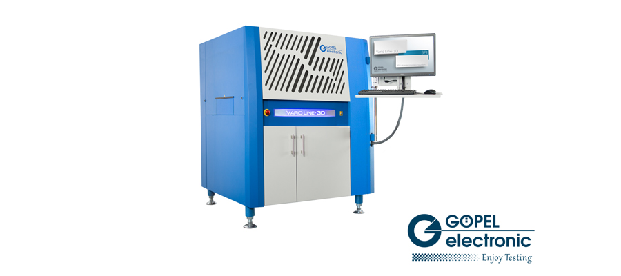
GÖPEL electronic presents with the new system Vario Line · 3D SPI an innovative system solution for the 3D inspection of solder and sintering pastes. The new system is based on the proven hardware platform of the AOI product family Vario Line. In particular, this achieves an extended inspection range and higher speed. At its heart is the high-speed 3D inspection module based on fringe projection, which ensures maximum reliability and reproducibility thanks to its advanced technology. With the Vario Line · 3D SPI, it is not only possible to assess the quality of the solder paste print, but also to inspect sintered pastes with structure heights of only 30 µm. In addition, a closed loop interface enables direct networking to paste printers or placement machines.
The Vario Line · 3D SPI has a link to PILOT Connect, the uniform networking system for all inspection data from AOI, SPI and AXI. This common interface ensures the central recording and management of the machine and operating data of all connected inspection systems. All inspection information can thus be brought together on one verification and repair station, which opens up secure error assessment and completely new possibilities for optimising the production process. In addition, the AI advisor software module, as an AI-based assistance function of the verification software, offers further options for reducing manufacturing efforts.
“The reliable detection and evaluation of criteria for printed pads such as height, area, volume, offset and paste bridges is an essential building block for ensuring the quality of assembled PCBs produced in SMD lines,” says Dr. Jörg Schambach, product manager for SPI systems at GÖPEL electronic. “But the Vario Line · 3D SPI is much more than just a system for defect detection. The great potential of solder paste inspection lies in the fact that process fluctuations can be automatically corrected by networking with other systems in the SMD production line. This ultimately leads to the best possible optimised production process in which product quality is permanently increased.”


