")
Courtesy: Lam Research
Lam Research is setting the agenda for the wafer fabrication equipment industry’s approach to a silicon photonics revolution, driving the breakthroughs in Speciality Technologies that will enable sustainable AI scaling through precision optical manufacturing.


The artificial intelligence boom has created an energy crisis that threatens to consume more electricity than entire nations. As data centres race to keep pace with AI’s insatiable appetite for computational power, technology leaders like Lam are shaping a fundamental shift that could redefine how we think about high-performance computing. One solution lies in replacing the electrical interconnects that have powered computing for decades with something far more efficient: light.
AI’s Energy Crisis: Why Power Demand Is Surging in Data Centres
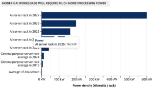
Goldman Sachs projects a 160% increase in data centre power demand by 2030, reaching 945 terawatt-hours annually — equivalent to Japan’s entire electricity consumption.
The problem runs deeper than software inefficiency. According to Bloomberg, AI training facilities house hundreds of thousands of NVIDIA H100 chips, each drawing 700 watts, nearly eight times the power consumption of a large TV. Combined with cooling systems, some hyperscale facilities now require as much power as 30,000 homes, driving tech companies to seriously consider dedicated nuclear plants.
The Paradigm Shift
Meeting this challenge requires a fundamental change in how chips are designed and connected. Silicon photonics—using light to transmit data—has the potential to provide dramatic improvements in speed and efficiency over traditional electrical interconnects. Precision optical manufacturing makes this shift possible, enabling scalable processes that can support the next era of energy-efficient, high-performance computing.
Silicon photonics represents a fundamental reimagining of how data moves within computing systems. Instead of pushing electrons through copper wires, this technology uses photons—particles of light—to carry information through silicon waveguides that function like nanoscale fibre optic cables, integrated directly onto chips.
The efficiency gains are dramatic. Optical interconnects consume just 0.05 to 0.2 picojoules per bit of data transmitted, compared to the much higher energy requirements of electrical interconnects over similar distances. As transmission distances increase, even within a single package, the energy advantage of photonics becomes overwhelming.
TSMC has published several research papers on silicon photonics since late 2023. The company has announced public partnerships with NVIDIA to integrate optical interconnect architectures into next-generation AI computing products. Lam is leading the industry’s approach to the transition to silicon photonics. As a technology leader with deep expertise in precision manufacturing, we are defining the roadmap for silicon photonics production, working closely with leading foundries and fabless companies to address the unique challenges presented by optical interconnects.
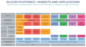
According to Yole Group, the market for silicon photonics is expected to grow from $95 million in 2023 to more than $863 million in 2029, with a 45% annual growth rate that reflects the technology’s expected rapid commercial adoption.
The Limits of Copper: Why Traditional Interconnects Can’t Scale With AI
At the heart of this energy crisis lies a fundamental bottleneck that has been building for years. While computing performance has advanced at breakneck speed, the infrastructure connecting these powerful processors has not kept pace. Hardware floating-point operations (FLOPS) have improved 60,000-fold over the past two decades, but DRAM bandwidth has increased only 100-fold, and interconnect bandwidth just 30-fold over the same period.
This creates what engineers call the “memory wall,” a constraint where data cannot move between processors and memory fast enough to fully use the available computing power. In AI applications, where massive datasets must flow seamlessly between graphics processors, high-bandwidth memory, and other components, these interconnect limitations become critical performance bottlenecks.
The solution that worked for previous generations—simply shrinking copper interconnects and packing them more densely—is reaching physical limits. As these copper traces become smaller and more numerous, they consume more power, generate more heat, and introduce signal integrity issues that become increasingly difficult to manage. Each voltage conversion in a data centre’s power delivery system introduces inefficiencies, and copper interconnects compound these losses throughout the system.
Modern AI architectures require what engineers call “high access speeds within the stack.” Chips become thinner, interconnects evolve from through-silicon vias (TSVs) to hybrid bonding, and memory modules must connect directly to graphics processors at unprecedented speeds. But when that high-speed memory connection has to traverse copper tracks on a circuit board to reach another processor, much of the bandwidth advantage disappears.
Silicon Photonics Meets AI: Co-Packaged Optics for Next-Gen Performance
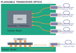
Silicon photonics is not entirely new; it has powered telecommunications networks for years through pluggable transceivers that connect data centre racks. These proven systems use silicon photonic dies combined with separate lasers and micro-lens technologies packaged into modules that can be easily replaced if they fail.
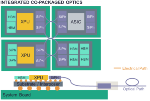
But AI’s demands are pushing photonics into uncharted territory. Instead of simply connecting separate systems, the technology must now integrate directly with processors, memory, and other components in what engineers call “co-packaged optics.” This approach promises to bring optical interconnects closer to the actual computation, maximising bandwidth while minimising energy consumption.
The challenge is reliability. While pluggable transceivers can be easily swapped out if they fail, co-packaged optical systems integrate directly with expensive graphics processors and high-bandwidth memory, making them a more reliable option. If an optical component fails in such a system, the repair becomes exponentially more complex and costly. Early implementations from major chip developers are still in pilot phases, carefully assessing long-term reliability before full-scale deployment.
Accelerating Adoption: How Industry Timelines Are Moving Faster Than Expected
Industry roadmaps that once projected capabilities for 2035 are already being met by leading manufacturers. The combination of urgent market need, massive investment, and three decades of accumulated photonics research has created what amounts to a perfect storm for commercialisation.
The implications extend far beyond data centres. As optical interconnects become more cost-effective and established, they have the potential to revolutionise everything from autonomous vehicles to edge computing devices. The same technology that enables sustainable AI scaling could ultimately transform how electronic systems communicate across virtually every application.
The Future of Computing Is Optical Interconnects for Sustainable AI Growth
The question is how quickly it can be implemented and scaled. With leading manufacturers already investing billions and pilot systems entering data centres, the light-speed future of computing is no longer a distant possibility. Companies like Lam, through our customer-centric approach and advanced manufacturing solutions, enable this transformation by providing the precision tools that make commercial silicon photonics possible.
Silicon photonics represents a fundamental technology shift that could determine which companies lead the next phase of the digital revolution. Just as the introduction of copper interconnects enabled previous generations of performance scaling, optical interconnects have the potential to break through the barriers that threaten to constrain AI development.
For an industry grappling with the sustainability challenges of exponential AI growth, silicon photonics offers a path forward that doesn’t require choosing between performance and environmental responsibility. By replacing electrical inefficiency with optical precision, this technology could enable the continued advancement of AI while dramatically reducing its environmental footprint.
The revolution is just beginning, but one thing is clear: the future of high-performance computing is increasingly bright, and Lam is at the centre of it.