Researchers at the Tyndall National Institute (Cork, Ireland) are developing a next-generation passive optical network (PON) demonstration module for high-speed fiber-to-home internet connectivity as part of the European FP7-Project “FABULOUS.” At the heart of the PON is a silicon photonic integrated circuit (Si-PIC) that receives information on an incoming optical-signal (downloading), before reflecting the optical signal back, after encoding extra information (uploading).
In this device, an electronic integrated circuit (EIC) is bonded to the top of the Si-PIC to distribute the electronic timing signals that are needed to drive the optical modulator in the photonic chip. Joule-heating from these high-frequency timing-signals causes an increase in the temperature of the EIC and Si-PIC, which can have a significant impact on the performance and reliability of the photonic chip.
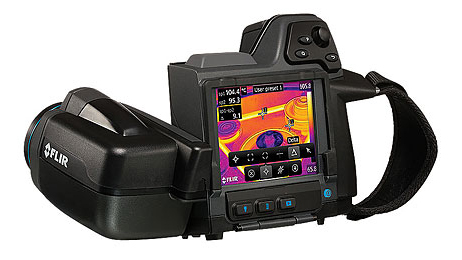
To image the silicon-photonic optical network unit (ONU) and to visualize and measure its heat output, the Tyndall researchers are using a thermal microscope system that includes a FLIR Systems (Meer, Belgium) X6540sc thermal imaging camera, allowing the researchers to simultaneously measure the EIC and Si-PIC temperatures in different operating modes so that they can chose the most efficient way to thermally stabilize the photonic chip.
“The last decade has seen the emergence of silicon photonics as a vehicle for next-generation information communication technology applications,” says Lee Carroll, research manager at the Photonics Packaging Group at Tyndall. “The need for high-performance optoelectronic devices is driven by an ever-increasing demand for higher bandwidth in data and telecom networks. One practical solution for the efficient distribution of high-speed electrical modulation onto the photonic platform is the face-to-face stacking (3D-integration) of a driver electronic integrated circuit on top of a silicon photonic integrated circuit (Si-PIC).”
“The thermal behavior of a packaged Si-PIC can impact the performance, stability, and lifetime of the device,” adds Kamil Gradkowski, another researcher at the Packaging Group. “We use a combination of thermal modelling and temperature measurements to characterize the thermal behaviour of a packaged PIC. Being able to conduct high-resolution (640 x 512 pixel) thermal measurements at high frame rates (100 Hz) using the FLIR X6540sc camera has shown that thermal management of the photonic module accounts for approximately 30% of the overall power budget, and so is a significant factor in the overall operational cost. We aim to use the camera to evaluate future packaging designs that are better optimized for cooling.”


