
CEA-Leti, the coordinator of the FAMES Pilot line, has achieved a major milestone for next-generation chip stacking: fully functional 2.5 V SOI CMOS devices fabricated at 400°C. The devices match electrical performance of devices fabricated at standard thermal budget (>1000 °C), removing one of the last barriers to large-scale 3D sequential integration (3DSI) —a core objective of FAMES.
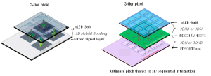
Enabled by advanced CEA-Leti expertise in low-temperature processes (nanosecond laser annealing (NLA) and solid-phase epitaxy regrowth (SPER)), this work offers true three-dimensional device stacking from the lab to fab. 3D sequential-integration interconnection density between tiers is the highest among 3D technologies, such as TSV and hybrid bonding. In this project, CEA-Leti demonstrated that Si CMOS is BEOL compatible, and thus can be stacked safely above BEOL, while transistor performance and maturity overtake largely the other technological options from the state-of-the-art, low-temperature solutions.


The achievement, presented today in a paper at IEDM 2025, titled, “High Performance 2.5 V n&p 400 °C SOI MOSFETs: A Breakthrough for Versatile 3D Sequential Integration,” is a key breakthrough for the FAMES Pilot Line, a European Union initiative launched in 2023 in response to the EU Chips Act strategy to strengthen sovereignty and competitiveness in semiconductor technologies. By combining 3D heterogeneous and sequential integration on FD-SOI platforms, the consortium aims to enable a new generation of More-Than-Moore devices and applications.
Enabling New Chip Architectures
“This breakthrough is a major milestone of the FAMES project as it enables innovative new chip architectures,” said Dominique Noguet, CEA-Leti vice president and coordinator of the FAMES Pilot Line. “Our low-temperature process could accelerate real-world demonstrations of multi-tier stacks combining advanced CMOS logic, with smart pixel or RF layers, to create new high-performance 3D chips.”
The team showed that SOI devices processed at 400 °C instead of the high temperature (>1000 °C) industry standard and high-temperature industrial reference, performed equivalent to high-temperature devices.
“The 400 °C process enables 3D sequential stacking on any bottom tier,” Noguet said. “It’s a huge step forward because it’s far more mature—reliable and scalable—than current low-temperature solutions, such as polycrystalline films, oxide semiconductors or carbon nanotubes.”
Protecting Circuitry on Bottom-Tier Layers
CEA-Leti’s team demonstrated n- and p-type transistors matching the characteristics of conventional high-temperature CMOS devices, while staying within the ≤400 °C thermal budget required to preserve active circuitry in lower layers.
The process relies on an optimized 400 °C LPCVD deposition for amorphous silicon followed by NLA in the melt regime for dopant activation and diffusion—producing polycrystalline, low-resistance gates with excellent interface quality. In addition, NLA-SPER mastering enables dopant activation without diffusion leading to access resistance within specifications.