Courtesy: Ayar Labs
Optical interconnect is used to generate, process, and manipulate light for faster data transmission, both between and within microelectronic chips. In a typical electro-optical transceiver, electronic data is converted into an optical signal and vice versa. Before the invention of silicon photonics, photonic components such as lasers, modulators, photon detectors, waveguides, and transimpedance amplifiers were built using discrete components, each fabricated in an exotic and costly process technology. Not only that, these discrete photonic components were bulky, and due to the relatively long traces separating them, significant power was required to connect them in an MCM (multi-chip module). Silicon photonics changes this picture. Silicon photonics is an innovation allowing photonic components (except the lasers) to be fully integrated or fabricated onto a common silicon substrate using widely available, inexpensive CMOS process technology. From the early proofs of principles in the 1980s, silicon photonics has evolved from discrete optical devices on chips to hybrid integration and monolithic integration in the 2010s. “PIC” (photonic integrated circuit) is often used to denote a photonic chip containing photonic components.
Ayar Labs goes one step further. Its TeraPHY™ in-package optical I/O chiplet integrates not only a PIC, but also an EIC (electric integrated circuit) that contains all electrical components in an electro-optical transceiver. Examples of electrical components include clock-data recovery (CDR), serializer, deserializer, equalizer, driver, and sampler. Ayar Labs’ optical I/O chiplet is therefore a fully integrated electro-optical transceiver offering high cost, power, and latency benefits.
Due to technological advantages, below are five reasons why silicon photonics is a key technology to address the ubiquitous computing bandwidth bottleneck problem across multiple market segments.
- Compatibility with CMOS Process Technology
Ayar Labs’ optical I/O chiplet, built with silicon photonics, enables, extends, and increases data transmission. Optical I/O chiplets consume less power and generate less heat than conventional electronic circuits, offering the promise of energy-efficient bandwidth scaling. Silicon photonics is compatible with CMOS fabrication, which allows silicon photonic devices to be manufactured using established foundry infrastructure. Given the physics of photonics, prior-generation CMOS nodes are perfectly suitable to pattern and fabricate the photonic devices and circuits.
- Bridging the Power Supply
Lasers are light sources that provide optical energy to photonic components. Lasers are not possible in silicon process technology since silicon is an indirect bandgap material. For light to be generated, a process material with a direct bandgap is needed. This requirement can be fulfilled in a III-V material such as indium phosphide (InP) that is commonly used to create semiconductor lasers for the wavelengths used in telecom and datacom (1550 and 1310nm).
Ayar Labs has developed an external light source (ELS) module, the SuperNova™ light source, that provides optical energy to the electro-optical TeraPHY™ transceivers. The SuperNova light source is compliant with the CW-WDM MSA (Continuous Wave-Wavelength Division Multiplexing Multi-Source Agreement) standard and presently can support 8 wavelengths. See Figure 1. Applications based on WDM-based transceivers benefit from significantly more bandwidth in each I/O fiber cable.
- Packaging Within a Chiplet
Thousands of different components must be integrated in a silicon photonics chiplet, including the modulator that translates data into photons, the waveguide that transports light around the integrated circuit (IC), and the photon detector that converts photons to electrons to be processed. These photonic components must be miniature in size to fit into an IC or chiplet form factor. The microring modulator used in Ayar Labs’ optical I/O chiplet is a critical component because it is about one-hundredth the size of a Mach-Zehnder modulator (MZM).
- Addressing the “Power Wall” Issue
Data movement is power hungry. As data centers demand higher bandwidth, electrical data rates must increase, and the power consumption required to move data through copper cables becomes unsustainable. As seen in Figure 3, the power required for off-chip electrical I/O is presently exceeding the total power allowed in the package, an issue known as the “Power Wall.” A silicon photonics chiplet is needed to alleviate this problem since it consumes only a fraction, about 20 percent, of today’s I/O power. We want to use the available power for data processing and not for data transport.
- Enabling Disaggregated Architectures
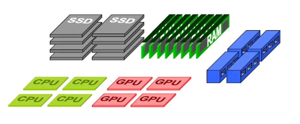
Given that optical I/O chiplets can move data over long distances up to a few hundred meters with only a minor degradation in signal integrity, silicon photonics is a key technology to enable disaggregated architectures in data centers where resources such as CPUs, GPUs, and memory storage can be separated within a rack or across racks. See Figure 4. Depending on the complexity of the workloads, these software-configurable resources are then pulled together to perform the tasks. The key benefit here is better utilization of available resources, resulting in better total cost of ownership (TCO).


