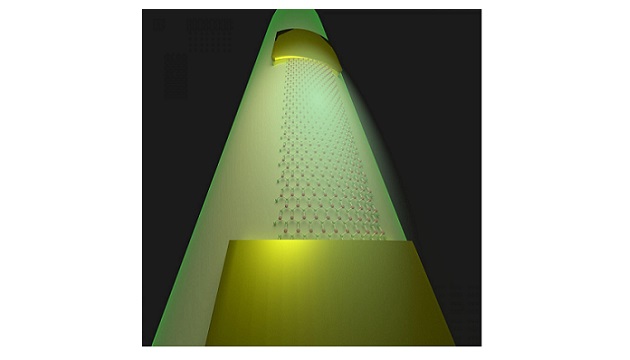
Atom-flat sensors, made from 2D materials, could be used to monitor performance without adding weight or hindering signal flow if they could be seamlessly integrated onto surfaces with different geometries where detection for near-field signal is desired.
2D materials are often touted for their strength, but it’s difficult to move 2D materials without damaging them. Researchers at Rice University have devised a way to keep the materials and their associated circuitry, including electrodes, intact as they’re moved to curved or other smooth surfaces.
To test their concept, the researchers made a 10-nm-thick indium selenide photodetector with gold electrodes and placed it onto an optical fiber. The near-field sensor effectively coupled with an evanescent field (the oscillating electromagnetic wave that rides the surface of the fiber) and accurately detected the flow of information inside the fiber.
Before moving the raw 2D materials to the optical fiber, the researchers covered the materials with a protective layer of polymethyl methacrylate (PMMA, commonly known as plexiglass). A robust bottom layer for the materials was also needed to keep the circuit intact during the move. Both the top and bottom layers needed to be removable.
The ideal solution for the bottom layer, according to the Rice team, was polydimethylglutarimide (PMGI), a sacrificial material used in micromachining. PMGI can be used as a device fabrication platform and easily etched away before transfer to the target. “We’ve spent quite some time to develop this sacrificial layer,” professor Jun Lou said. The researchers found that PMGI also worked with molybdenum diselenide (MoSe2) and other 2D materials.
The device transfer technique developed by the team utilizes the sacrificial polymer underlayer to achieve clean and nondestructive full device transfer. The researchers demonstrated their technique by transferring a complete 2D multilayer InSe photodetector device onto a stripped optical fiber.
Their superthin flexible device assemblies can be integrated onto the fibers themselves to noninvasively monitor the optical fiber performance, the researchers said. The demonstration of optically coupled, conformal 2D devices on substrates of different form factors could enable a variety of near-field optical and sensing applications.
“This paper proposes several interesting possibilities for applying 2D devices in real applications,” Lou said. “For example, optical fibers at the bottom of the ocean are thousands of miles long, and if there’s a problem, it’s hard to know where it occurred. If you have these sensors at different locations, you can sense the damage to the fiber.”


