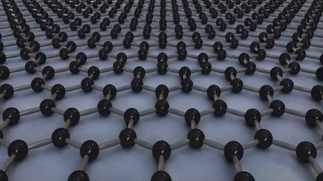
Palladium diselenide shows promise in electronics and photonics. By exfoliating bulk crystals of palladium(IV) selenide, chemists have prepared the first ever pentagonal 2D material. Palladium and selenium atoms form a Cairo pentagonal tiling pattern, an unusual arrangement that gives the new material interesting electronic properties, similar to other non-symmetrical 2D materials like phosphorene.
Kai Xiao from Oak Ridge National Laboratory in Tennessee, US, explains that his group was attracted by palladium diselenide’s ‘unique puckered pentagonal building blocks, unsimilar to current 2D materials’.
Xiao’s team first built bulk crystals by melting stoichiometric amounts of palladium and selenium in a furnace. Then, as with the preparation of graphene sheets, they used micromechanical exfoliation to obtain the thin layers of palladium selenide. They used atomic-resolution scanning transmission electron microscopy (AR-STEM) to visualise the unique pentagonal tiling.
To measure the band gap of this new semiconductor, Xiao and colleagues performed both micro-absorption optical spectroscopy and DFT computational calculations. Experiments showed the band gap can be tuned from 0 eV for bulk PdSe2 to 1.3 eV for the monolayers. This indicates it is an ‘excellent semiconductor which can absorb light for electronic and optoelectronic devices, such as transistors, solar cells, [or] photodetectors’, Xiao explains. Alessandro Molle, an expert on 2D-xenes in the National Research Council of Italy, agrees. ‘Being not far from silicon, the band gap of 1.3 eV is satisfactory for electronic applications where two logic states must be sharply discriminated, namely digital devices or logic switches,’ he says, adding that further studies ‘should make clear what is the real benefits against other ultra-thin or 2D competitor’.
Antonio Helio Castro-Neto, director of the Centre for Advanced 2D Materials at the University of Singapore, explains that palladium diselenide’s band gap is ‘very attractive for electro-optical applications, but this is not unique’. He highlights the true importance of this discovery relies on ‘the stability of this material in air, something that many 2D semiconductors don’t show’.
Molle points out the exceptionality of the pentagonal arrangement in PdSe2. ‘So far, no evidence of a pentagonal arrangement has been clearly stated since now, he says. Xiao agrees Cairo tiling patterns are scarce in nature. ‘I only found them in [columnar basalt formations] like the Giant’s Causeway in [Northern] Ireland,’ he says. These unusual structures ‘may pave the way to a new structural fashion of emerging 2D materials and may have important implication on the chemistry to play with in the synthetic stage,’ Molle says. ‘More is yet to come on the scalability of PdSe2 production, but I’d say [it will] foster intense research.’
Source: ChemistryWorld


